
Chip and packaging method thereof

A chip packaging and chip technology, applied in the field of chips and their packaging, can solve problems such as high cost and many process flows, and achieve the effects of reducing packaging costs, reducing packaging process flows, and eliminating the reconfiguration of chip position accuracy.

Inactive Publication Date: 2017-05-31
NAT CENT FOR ADVANCED PACKAGING
View PDF5 Cites 2 Cited by
  • Summary
  • Abstract
  • Description
  • Claims
  • Application Information

AI Technical Summary

Problems solved by technology

[0005] The embodiment of the present invention provides a chip and its packaging method to solve the problems of many process flows and high cost in the existing packaging technology

Method used


Image

  • Chip and packaging method thereof
  • Chip and packaging method thereof
  • Chip and packaging method thereof

Examples


Embodiment Construction

[0036] In order to make the purpose, technical solutions and advantages of the present invention clearer, the technical solutions of the present invention will be clearly and completely described through implementation with reference to the accompanying drawings in the embodiments of the present invention. Obviously, the described embodiments are the embodiment of the present invention. Some, but not all, embodiments. Based on the embodiments of the present invention, all other embodiments obtained by persons of ordinary skill in the art without making creative efforts belong to the protection scope of the present invention.

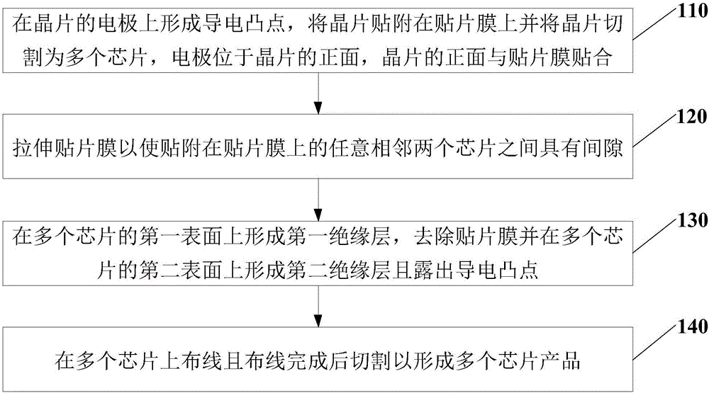
[0037] figure 1 It is a flowchart of a chip packaging method provided by an embodiment of the present invention. The chip packaging method provided in this embodiment specifically includes the following steps:

[0038] Step 110 , forming conductive bumps on the electrodes of the wafer, attaching the wafer to the chip, and cutting the chip into multiple...


PUM


Abstract

The embodiment of the invention discloses a chip and a packaging method thereof. The chip packaging method comprises the following steps: forming conductive salient points on an electrode of a wafer, attaching the wafer to a patch film, and cutting the wafer into a plurality of chips, wherein the electrode is positioned on the front side of the wafer, and the front side of the wafer is laminated with the patch film; stretching the patch film, so that a gap is formed between any two adjacent chips attached to the patch film; forming first insulation layers on first surfaces, which face away from the patch film, of the plurality of chips, removing the patch film, forming second insulation layers on second surfaces, which face the patch film, of the plurality of chips, and exposing the conductive salient points; wiring on the plurality of chips and cutting the plurality of chips after finishing the wiring to form a plurality of chip products. By adopting the chip and the packaging method thereof in the embodiment of the invention, the packaging process flow is reduced, the packaging cost is lowered, and the problem of poor position accuracy of a reconstructed chip caused by surface mounting process errors is solved.

Description

technical field [0001] Embodiments of the present invention relate to chip packaging technology, and in particular to a chip and a packaging method thereof. Background technique [0002] With the rapid development of multi-functionalization and miniaturization of electronic products, high-density microelectronic assembly technology has gradually become the main assembly technology of electronic products. In order to cooperate with the development of electronic products, especially smart phones, handheld computers, ultrabooks and other products, the size of the chip is developing in the direction of higher density, faster speed, smaller size and lower cost, so the packaging technology of the chip is also becoming more and more more important. The existing chip packaging technology is mainly wafer-level packaging technology. [0003] When using wafer-level packaging technology to package chips, firstly, the cut chips are pasted on the carrier sheet through the adhesive film,...

Claims


Application Information

Patent Timeline
IPC IPC(8): H01L21/56H01L23/31H01L23/488H01L21/60
CPCH01L21/56H01L23/31H01L23/488H01L24/02H01L24/03H01L24/10H01L24/11
Inventor 陈峰陆原
Owner NAT CENT FOR ADVANCED PACKAGING
Learn More