Antenna packaging structure and packaging method

An encapsulation method and technology of encapsulation structure, which are applied in the directions of antenna support/installation device, antenna grounding switch structure connection, and antenna, etc., can solve the problems such as the difficulty of effective protection of the chip and the large size of the antenna encapsulation, and reduce the encapsulation process flow, The effect of high efficiency antenna performance and high process structure integration

Pending Publication Date: 2021-04-27
SJ SEMICON JIANGYIN CORP
View PDF0 Cites 0 Cited by
  • Summary
  • Abstract
  • Description
  • Claims
  • Application Information

AI Technical Summary

Problems solved by technology

[0006] In view of the above-mentioned shortcomings of the prior art, the object of the present invention is to provide an antenna packaging structure and packaging method, which are used to solve the problems in the prior art that the antenna packaging volume is large and the chip is difficult to be effectively protected.

Method used


Image

  • Antenna packaging structure and packaging method
  • Antenna packaging structure and packaging method
  • Antenna packaging structure and packaging method

Examples


Embodiment 1

[0083] Such as figure 1 As shown, the present invention provides a kind of antenna packaging method, and described packaging method comprises steps:

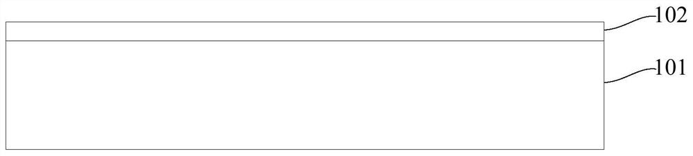
[0084] providing a support base on which a temporary bonding layer is formed;

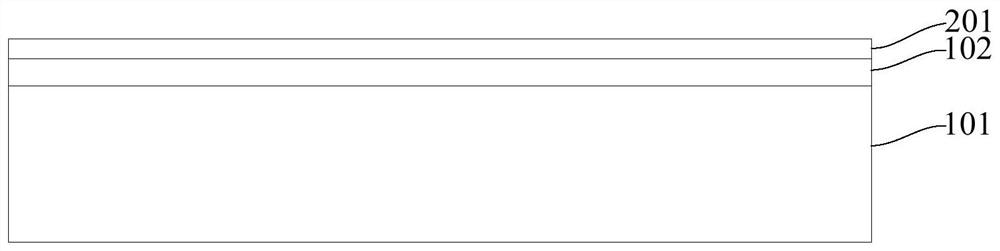
[0085] forming a rewiring layer on the temporary bonding layer, the rewiring layer including a first surface connected to the temporary bonding layer and a second surface opposite to the first surface;

[0086] forming a first antenna layer electrically connected to the redistribution layer on the second surface;

[0087] forming a metal feeder post electrically connected to the first antenna layer on the first antenna layer;

[0088] encapsulating the metal feeder column with an encapsulation layer, and exposing the top surface of the metal feeder column by the encapsulation layer;

[0089] forming a second antenna layer electrically connected to the metal feeder post on the encapsulation layer;

[0090] providing at least one semiconductor chip...

Embodiment 2

[0120] Such as Figure 16 shown, and see Figures 1 to 15 , the present invention also provides an antenna packaging structure, wherein the antenna packaging structure is preferably packaged by the antenna packaging method of the present invention, of course, the antenna packaging structure can also be packaged by other packaging methods, the antenna package Structures include:

[0121] a rewiring layer comprising a first side and a second side opposite to the first side;

[0122] The first antenna layer 301 is formed on the second surface and is electrically connected to the rewiring layer;

[0123] a metal feeder post 303 formed on the first antenna layer 301 and electrically connected to the first antenna layer 301;

[0124] An encapsulation layer 305, covering the metal feeder post 303, the encapsulation layer exposing the top surface of the metal feeder post 303;

[0125] The second antenna layer 307 is formed on the encapsulation layer 305, and the second antenna lay...


PUM


Abstract

The invention provides an antenna packaging structure and a packaging method. The packaging method comprises the steps of providing a supporting substrate, forming a rewiring layer, a first antenna layer, a metal feeder column, a packaging layer and a second antenna layer, providing a semiconductor chip, enabling the semiconductor chip to be connected to the surface of the second antenna layer, and forming a box dam dispensing protection layer at least at the top and periphery of the semiconductor chip. A box dam dispensing process is added to wafer-level packaging, the stability of the chip is improved, a bottom filling layer is further formed through a bottom filling process, dual protection is carried out on the chip, the packaging process flow can be effectively reduced, all active components or passive components are integrated in one packaging structure, the packaging size can be effectively reduced, the semiconductor chip, the rewiring layer, the antenna metal and other structures are arranged in a vertical arrangement structure, the conduction path between components can be effectively shortened, the power consumption is low, the integration of the process structure is high, the signal receiving capability can be enhanced by adopting the multi-layer antenna arrangement, and the signal receiving bandwidth can be expanded.

Description

technical field [0001] The invention belongs to the field of packaging and the field of communication equipment, and in particular relates to an antenna packaging structure and a packaging method. Background technique [0002] Due to the progress of science and technology, various high-tech electronic products have been developed to facilitate people's life, including various electronic devices, such as notebook computers, mobile phones, tablet computers (PADs), and the like. [0003] With the popularization of these high-tech electronic products and the increase of people's demand, in addition to the substantial increase of various functions and applications configured in these high-tech products, especially in order to meet people's mobile needs, the function of wireless communication has been added. Therefore, people can use these high-tech electronic products at any place or at any time through these high-tech electronic devices with wireless communication functions. Th...

Claims


Application Information

Patent Timeline
Patent Type & Authority Applications(China)
IPC IPC(8): H01L23/66H01L21/48H01L21/56H01L21/768H01L23/31H01L23/498H01L23/538H01Q1/22H01Q1/38H01Q1/50
CPCH01L23/66H01L21/4853H01L21/76895H01L21/56H01L23/3114H01L23/49838H01L23/49811H01L23/5386H01Q1/2283H01Q1/38H01Q1/50H01L2224/16225H01L2224/73204H01L2224/32225H01L2924/00
Inventor 黄晗林正忠吴政达陈彦亨
Owner SJ SEMICON JIANGYIN CORP
Why Eureka
Try Eureka