
LED flip chip integrated packaging structure and packaging method thereof

An integrated package and chip technology, which is applied in the field of LED flip-chip integrated package structure and its package, can solve the problems of large terminal LED products, achieve the effects of reducing the packaging process, increasing luminous efficiency, and reducing the cost of packaging materials

Pending Publication Date: 2019-07-12
CHANGZHOU INST OF TECH RES FOR SOLID STATE LIGHTING
View PDF0 Cites 0 Cited by
  • Summary
  • Abstract
  • Description
  • Claims
  • Application Information

AI Technical Summary

Problems solved by technology

[0007] In order to solve the problem that the LED drive circuit cannot be integrated on the LED chip package in the prior art, resulting in a large volume of terminal LED products, a LED flip-chip integrated packaging structure is proposed. The invention provides an LED flip-chip integrated packaging structure that can Solve the problem of large volume of terminal LED products

Method used


Image

  • LED flip chip integrated packaging structure and packaging method thereof
  • LED flip chip integrated packaging structure and packaging method thereof
  • LED flip chip integrated packaging structure and packaging method thereof

Examples


Embodiment 1

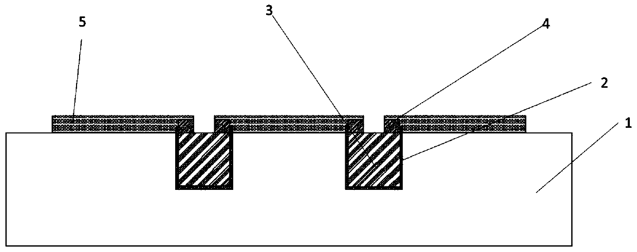
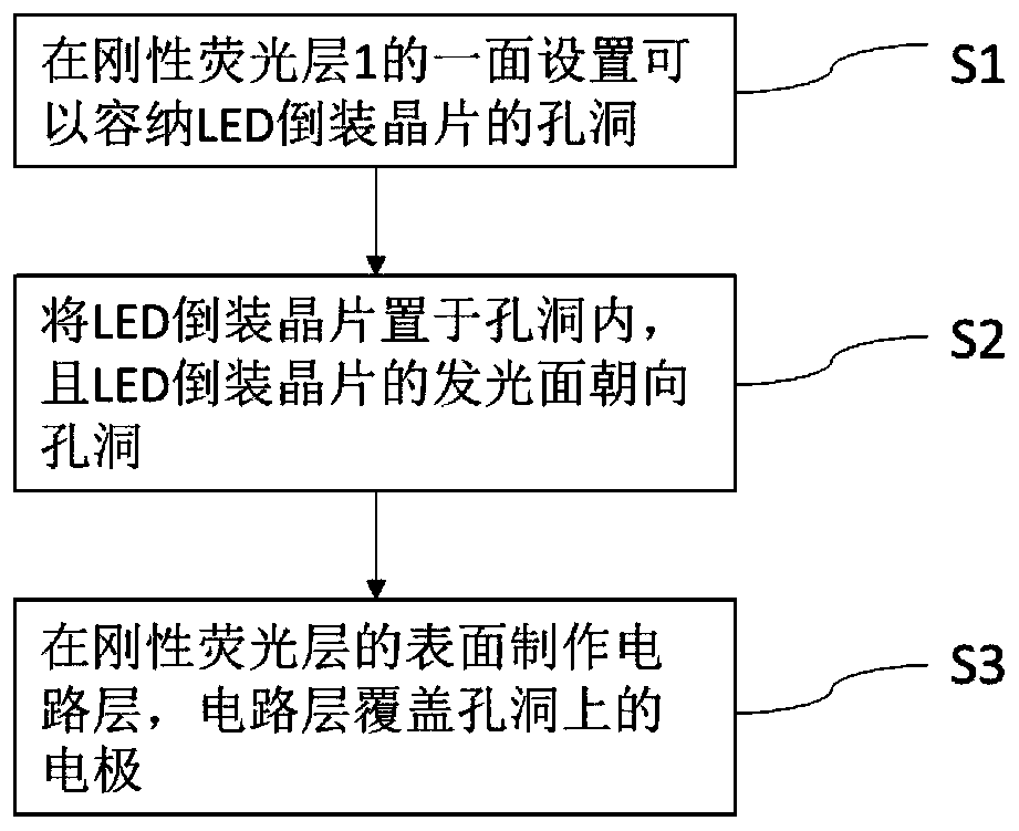
[0037] Such as figure 2 Shows the structural diagram of the LED flip-chip integrated packaging structure of the embodiment of the present invention, the LED flip-chip integrated packaging structure includes a rigid fluorescent layer 1, an LED flip-chip and a circuit layer 5, wherein the rigid fluorescent layer 1 is used as a packaging material, The packaging material is a material with high refractive index and light transmittance, such as ceramic fluorescent sheet, glass fluorescent sheet, single crystal silicon fluorescent sheet, etc., wherein the LED flip chip includes a light emitter 3 and an electrode 4, and the electrode 4 emits light The back of body 3.

[0038] Specifically, one side of the rigid phosphor layer 1 is provided with a hole for accommodating LED flip chip, the illuminant 3 is placed in the hole of the rigid phosphor layer 1, and the circuit layer 5 is arranged on the surface of the rigid phosphor layer 1 and covers the holes on the hole. The electrode an...

Embodiment 2

[0054] The embodiment of the present invention also provides an LED flip-chip integrated packaging structure, the principle is the same as the above-mentioned embodiment, the difference is that the circuit layer 5 is replaced by a reflective layer, and the reflective layer completely covers the rigid fluorescent layer 1 with a On one side of the hole (electrode 4 is not covered), the reflective layer is not connected to the electrode of the LED flip chip, and the electrode of the LED flip chip is connected to the driving circuit outside the integrated package structure. The luminous efficiency of the LED product can be better increased through the reflective layer .


PUM


Abstract

The invention discloses an LED flip chip integrated packaging structure and a packaging method thereof. The structure comprises a rigid fluorescent layer, an LED flip chip and a circuit layer. One side of the rigid fluorescent layer is provided with a hole for accommodating the LED flip chip. The LED flip chip includes an illuminant and an electrode, the electrode is on a back surface of the illuminant, and the illuminant is placed in a hole of the rigid fluorescent layer. The circuit layer is disposed on a surface of the rigid fluorescent layer, and the circuit layer is coupled to the electrode of the LED flip chip. The invention provides the LED flip chip integrated packaging structure and the packaging method thereof, the problem of the large size of a terminal LED product can be solved, the problem of the difficult heat radiation of an existing packaging method can be solved, and the problem that a wafer and positive and negative electrodes of a substrate / bracket are connected by using gold wire in an existing packaging mode and the LED chip fails to work normally due to the easy breaking of the gold wires can be solved.

Description

technical field [0001] The invention relates to the field of LED flip-chip packaging, in particular to an LED flip-chip integrated packaging structure and a packaging method thereof. Background technique [0002] At present, the existing technology of LED packaging mostly adopts figure 1 The structure is packaged, that is, at least one LED chip b is installed on the substrate / support a, and the LED chip b is fixed on the placement area on the substrate or support a by a die-bonding glue, and then the LED chip b and the substrate / support a are connected with gold wires The positive and negative poles of the package are connected to the circuit, and then the LED chip b and the gold wire are wrapped with fluorescent glue c and silica gel d, and finally baked to remove the air bubbles in the encapsulation glue to achieve isolation from the air and prevent moisture. However, the use of these two packaging methods has the following disadvantages: [0003] 1. Use gold wire to con...

Claims


Application Information

Patent Timeline
Patent Type & Authority Applications(China)
IPC IPC(8): H01L25/075H01L33/54H01L33/50H01L33/62H01L33/00
CPCH01L25/0753H01L33/54H01L33/50H01L33/62H01L33/005
Inventor 方涛侯君凯
Owner CHANGZHOU INST OF TECH RES FOR SOLID STATE LIGHTING
Features
  • Generate Ideas
  • Intellectual Property
  • Life Sciences
  • Materials
  • Tech Scout
  • Unparalleled Data Quality
  • Higher Quality Content
  • 60% Fewer Hallucinations
Learn More