

Double-layer convex-point diode chip preparation method
A diode and double-layer convex technology, which is applied in the field of double-layer bump diode chip preparation, can solve the problems of low yield and low efficiency, and achieve the effects of reducing packaging costs, high efficiency, and shortening the packaging process
- Summary
- Abstract
- Description
- Claims
- Application Information
AI Technical Summary
Problems solved by technology
Method used
Image

Examples
Embodiment Construction
[0013] The specific implementation method of the patent of the present invention is:
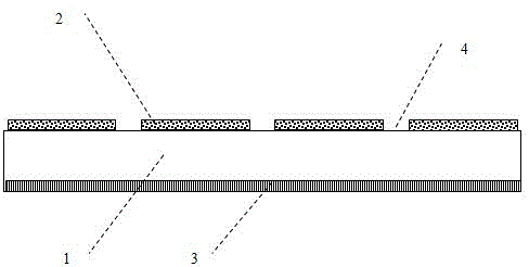
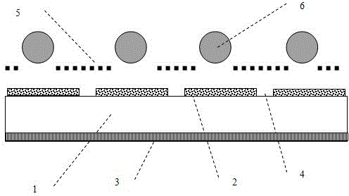
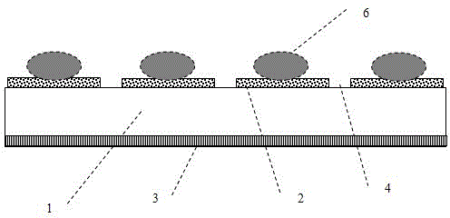
[0014] The schematic diagram of the structure of the semiconductor diode chip after metallization is completed. figure 1 shown, see figure 2 , punch the anode surface of the entire wafer, put the stencil 5 made according to the chip layout size on the wafer and align it, so that the position of the opening of the stencil corresponds to the bonding point of the anode 2 of each diode core one by one, Implant tin alloy balls 6 through the stencil 5 at the opening of the solder pad. The diameter of the tin alloy balls should be smaller than the size of the opening of the stencil. Remove the stencil, and heat the diode chip planted with balls to melt and reflow the tin alloy balls. After cooling, the tin alloy ball 6 forms an ohmic contact with the metal anode 2 of the diode chip, and forms an anode bump diode chip structure, see image 3 . Flip the anode bump diode chip so that the cathode ...
PUM
 Abstract
Description
Claims
Application Information