SiC MOSFET device with integrated schottky diode

A technology of Schottky diodes and Schottky metals, applied in semiconductor devices, electrical components, circuits, etc., can solve problems affecting device current density, increase in cell area, etc., and achieve improved switching performance, high integration and Density, reduced gate capacitance and the effects of input and output capacitance

Inactive Publication Date: 2017-05-31
BEIJING CENTURY GOLDRAY SEMICON CO LTD
View PDF4 Cites 21 Cited by
  • Summary
  • Abstract
  • Description
  • Claims
  • Application Information

AI Technical Summary

Problems solved by technology

The latest SiC MOSFET also integrates anti-parallel SBD in the device structure, and the integrated SBD is often made in the source region, such as the technical solution disclose

Method used


Image

  • SiC MOSFET device with integrated schottky diode
  • SiC MOSFET device with integrated schottky diode
  • SiC MOSFET device with integrated schottky diode

Examples


Embodiment Construction

[0024] The present invention will now be described more fully with reference to the accompanying drawings, in which exemplary embodiments of the invention are shown. This invention may, however, be embodied in many different forms and should not be construed as limited to the exemplary embodiments set forth herein. Rather, these embodiments are provided so that this disclosure will be thorough and complete, and will fully convey the scope of the invention to those skilled in the art.

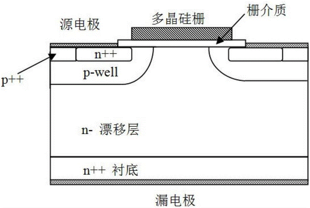
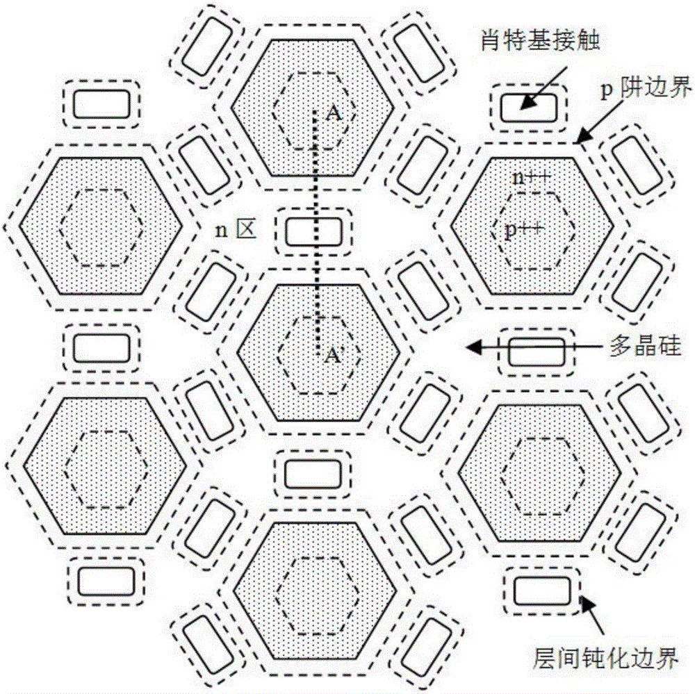
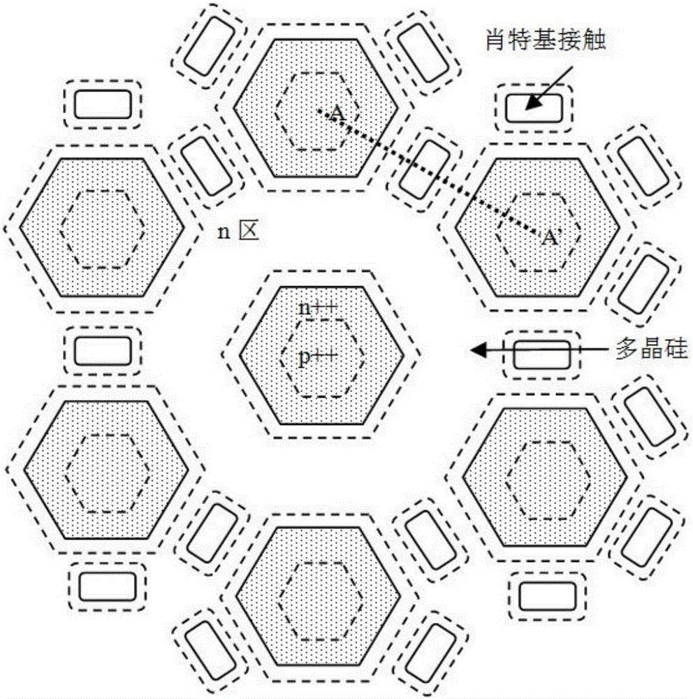
[0025] The whole device structure of the SiC MOSFET device of the present invention is composed of several parts such as an active area, a junction terminal area outside the active area, and a scribe groove. The active area is composed of many primary cells connected in parallel, and the source block metal and the gate block metal are finally formed in the active area, and the two are electrically isolated for subsequent packaging applications. The junction termination region can be in various ...


PUM

PropertyMeasurementUnit
Thicknessaaaaaaaaaa
Thicknessaaaaaaaaaa

Abstract

The invention discloses a SiC MOSFET device with an integrated schottky diode, wherein an original cell structure of a source region from top to bottom is a drain electrode, a substratum, a buffer layer, a drift layer and two P well regions symmetrically from the left and the right. The adjacent n++ area and P++ area arranged on the P well regions from left to right are sequentially provided with a source electrode, a grid electrode, a schottky metal, the grid electrode and the source electrode. The source electrode is positioned above the n++ area and P++ area. The surface part of the P well regions is fully covered with the grid electrode. One side of the grid electrode overlaps with the n++ area and the other side of the grid electrode overlaps with a JFET area. The schottky metal is positioned above the JFET area. The SiC MOSFET device with the integrated and inverse parallel schottky diode is provided, wherein the integrated schottky diode is located in the JFET area, adjacent to the grid electrode area. The SiC MOSFET device with higher original cell integration and density has the advantage of effectively utilizing the proportion of the JFET area. Meanwhile, compared with conventional MOSFET, the current MOSFET is capable of effectively reducing grid capacitance and input-output capacitance and improving switching performance of the device due to the area reduction of the gate capacitance.

Description

technical field [0001] The invention belongs to the field of semiconductors, and in particular relates to a SiC MOSFET device integrating Schottky diodes. Background technique [0002] SiC MOSFET After years of research in the industry, some manufacturers have taken the lead in launching commercial products. In many applications, controllable devices such as transistors need to be anti-parallel with a freewheeling diode to work together. For example, the commonly used silicon IGBT modules are anti-parallel fast recovery diodes as freewheeling diodes. If a freewheeling diode is integrated in a device, it not only improves the integration level of the chip, but also effectively reduces the cost of the chip. [0003] In order to suppress the opening of the internal parasitic BJT in the structure of modern MOSFET devices, the source and the p-well are often electrically connected and short-circuited. Therefore, modern SiC MOSFET devices often have anti-parallel pn diodes thems...

Claims


Application Information

Patent Timeline
IPC IPC(8): H01L29/78H01L29/06
CPCH01L29/0696H01L29/7827
Inventor 倪炜江
Owner BEIJING CENTURY GOLDRAY SEMICON CO LTD
Why Eureka
Try Eureka