Transistor laser and its manufacturing method

A transistor laser, base layer technology, applied in semiconductor lasers, lasers, laser parts and other directions, can solve problems such as unfavorable device optical devices or monolithic integration of electrical devices, and achieves omitting design and manufacturing steps, convenient integration, and easy integration. effect achieved

Active Publication Date: 2019-05-31
INST OF SEMICONDUCTORS - CHINESE ACAD OF SCI
View PDF4 Cites 0 Cited by
  • Summary
  • Abstract
  • Description
  • Claims
  • Application Information

AI Technical Summary

Problems solved by technology

[0003] However, the reported transistor lasers all require cleavage planes or distributed feedback mirrors with anti-multilayer structures to provide the necessary optical feedback to work, which is not conducive to monolithic integration of devices with other optical or electrical devices.

Method used


Image

  • Transistor laser and its manufacturing method
  • Transistor laser and its manufacturing method
  • Transistor laser and its manufacturing method

Examples


no. 1 example

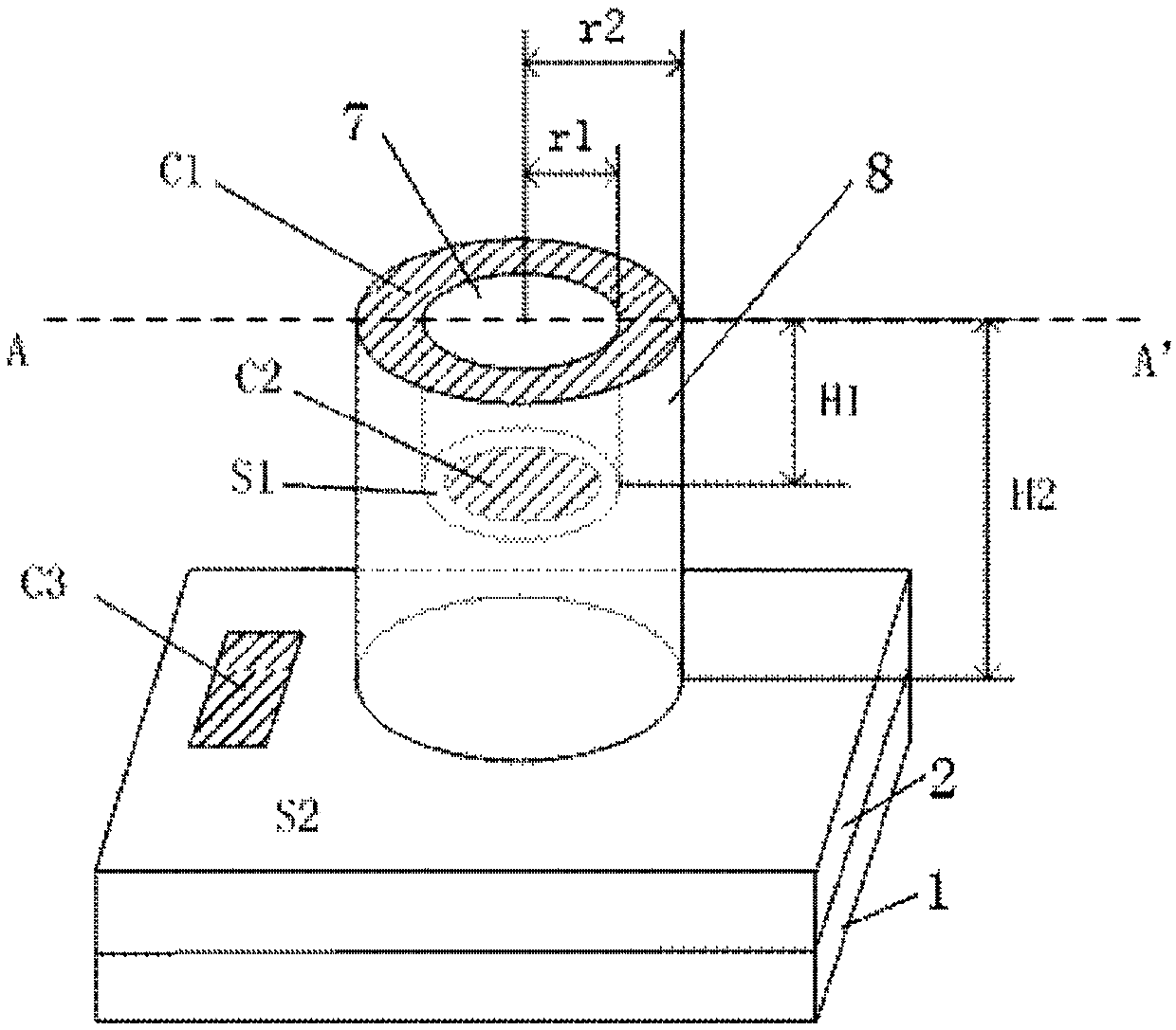
[0051] In a first exemplary embodiment of the present invention, a transistor laser and a fabrication method thereof are provided. figure 1 It is a schematic structural diagram of the transistor laser according to the first embodiment of the present invention. like figure 1 As shown, the transistor laser of this embodiment includes: a substrate 1, a lower collector layer 2, a columnar structure 8, and a columnar hole 7 disposed in the columnar structure 8, wherein the columnar structure 8 and the columnar hole 7 are both circular in cross section , and coaxially arranged, the first surface S1 is arranged at the bottom of the columnar hole 7, the second surface S2 is arranged on the surface of the lower collector layer, the emitter electrode C1 is arranged on the upper surface of the columnar structure 8, and the base electrode C2 is arranged on the upper surface of the columnar structure 8 On the first surface S1, the collector electrode C3 is disposed on the second surface S...

no. 2 example

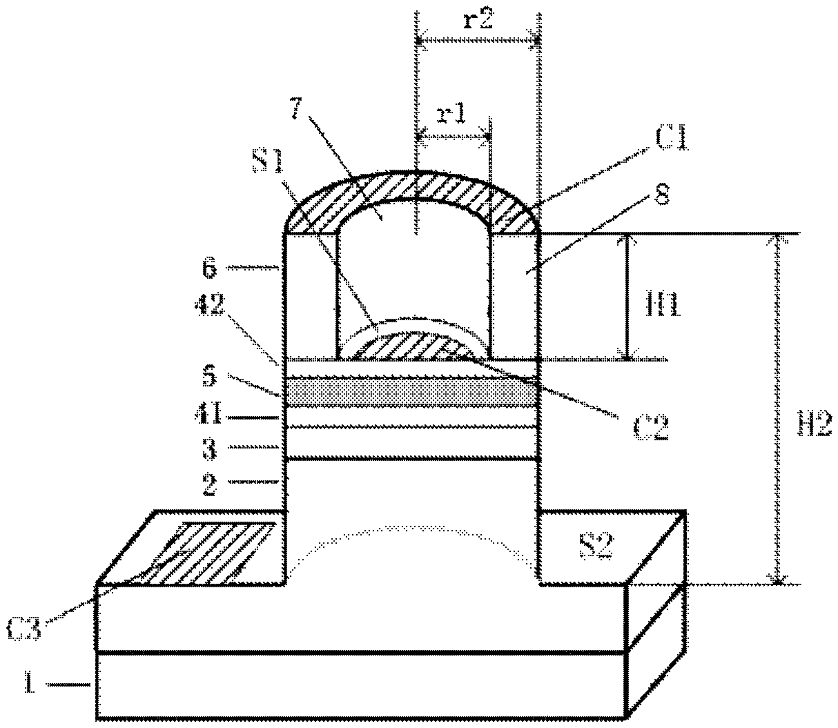
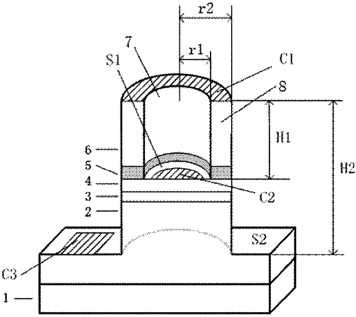
[0072] In a second exemplary embodiment of the present invention, a transistor laser and a fabrication method thereof are provided. and figure 1 Similarly, the transistor laser of this embodiment includes: a substrate 1, a lower collector layer 2, a columnar structure 8, and a columnar hole 7 disposed in the columnar structure 8, wherein the cross sections of the columnar structure 8 and the columnar hole 7 are both circular, And coaxially arranged, the first surface S1 is arranged at the bottom of the columnar hole 7, the second surface S2 is arranged on the surface of the lower collector layer, the emitter electrode C1 is arranged on the upper surface of the columnar structure 8, and the base electrode C2 is arranged at the bottom of the columnar hole 7. On one surface S1, the collector C3 is disposed on the second surface S2.

[0073] see image 3 , the transistor laser comprises from bottom to top: a substrate 1, a lower collector layer 2, a collector layer 3, a base lay...


PUM


Abstract

The invention provides a transistor laser device and a method for manufacturing the same, and belongs to the field of semiconductor laser devices. The transistor laser device is of a multilayer structure and sequentially comprises a substrate, a lower collector electrode layer, a collector electrode layer, a base layer and an emission layer from bottom to top. The base layer at least comprises a base electrode layer and a quantum well layer. The transistor laser device comprises an upper portion and a lower portion. The upper portion is of a columnar structure, and a boundary line of the columnar structure and the lower portion is positioned in the lower collector electrode layer; a columnar hole is formed in the columnar structure, the base layer is arranged at the bottom of the columnar hole, an emitting electrode is arranged on the upper surface of the columnar structure, a base electrode is arranged at the bottom of the columnar hole, and a collector electrode is arranged on the upper surface of the lower portion of the transistor laser device. The transistor laser device and the method have the advantages that feedback does not need to be provided via optical gratings or cleavage planes when the transistor laser device works, closed annular waveguide circuits formed by the columnar structure of the transistor laser device and the columnar hole are used as resonant cavities, and accordingly laser light can be resonated.

Description

technical field [0001] The invention relates to the field of semiconductor lasers, in particular to a transistor laser and a manufacturing method thereof. Background technique [0002] In 2005, a research team from the University of Illinois reported a semiconductor device called a heterojunction bipolar transistor laser [Appl.Phys.Lett.Vol.87, P.131103(2005).], only Using a relatively simple epitaxy and manufacturing process, the device simultaneously realizes the light emitting function of the laser and the amplification function of the transistor. The difference from ordinary transistors is that a quantum well is introduced in the base region of the transistor. Under a certain base-collector voltage, electrons will be injected into the base region from the collector region, and recombine with holes in the quantum well region to emit light. The light wave is reflected back and forth between the front and rear two cleavage cavity mirrors to be amplified, and after exceedi...

Claims


Application Information

Patent Timeline
Patent Type & Authority Patents(China)
IPC IPC(8): H01S5/34H01S5/343
CPCH01S5/34H01S5/343H01S5/34313
Inventor 梁松朱洪亮
Owner INST OF SEMICONDUCTORS - CHINESE ACAD OF SCI
Why Eureka
Try Eureka