Charge pump circuit, charge pump system and memory

A charge pump and circuit technology, which is applied in the field of charge pump system, memory and charge pump circuit, can solve the problem of reducing the area of ​​the charge pump circuit

Active Publication Date: 2017-05-31
SHANGHAI HUAHONG GRACE SEMICON MFG CORP
View PDF7 Cites 1 Cited by
  • Summary
  • Abstract
  • Description
  • Claims
  • Application Information

AI Technical Summary

Problems solved by technology

[0005] However, as the area requirements of the semiconductor process become higher and h

Method used


Image

  • Charge pump circuit, charge pump system and memory
  • Charge pump circuit, charge pump system and memory
  • Charge pump circuit, charge pump system and memory

Examples


Embodiment Construction

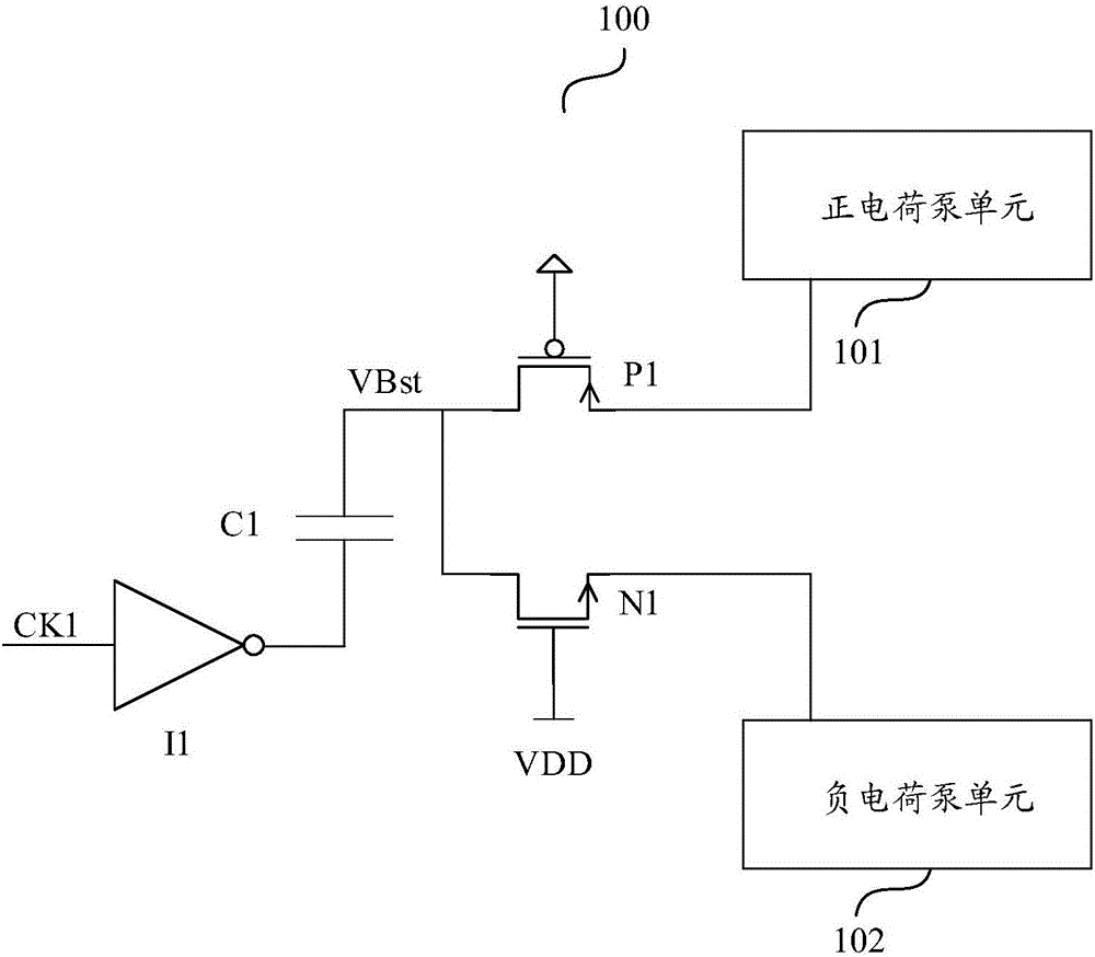
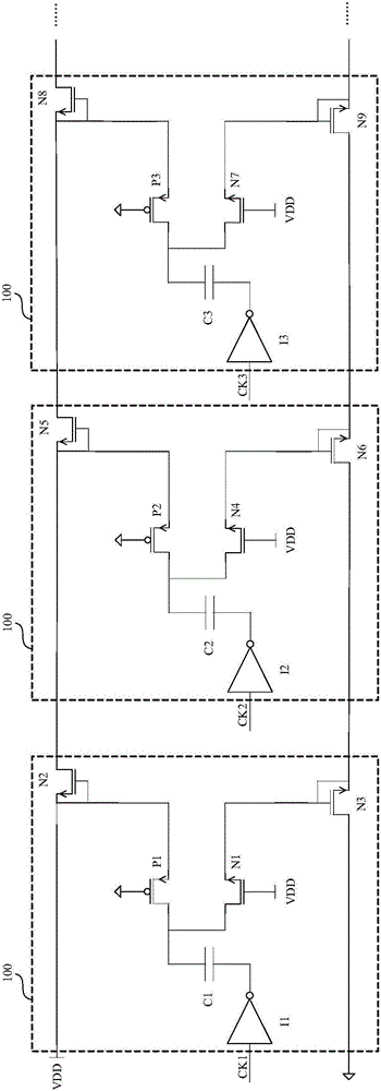
[0027] As mentioned in the background section, with the continuous development of semiconductor technology, the area of ​​the charge pump circuit in the prior art needs to be further reduced.

[0028] Continue to refer to figure 1, the inventor of the present application analyzed the charge pump circuit 100 . Since the working principle of the charge pump circuit 100 is that when the clock signal CK1 acts on the capacitor C1, while the capacitor C1 is boosted, the charge is transferred to the positive charge pump unit 101 and the negative charge pump unit 102, and the The phase of the clock signal CK1 and the positive charge pump unit 101 and the negative charge pump unit 102 determine whether to “store” or transmit the charge. According to the relationship Q=C×U of the capacitor C, the voltage U and the charge Q stored in the capacitor, it can be seen that when the charge stored in the capacitor is constant, the larger the applied voltage, the smaller the capacitor can be. ...


PUM


Abstract

The invention discloses a charge pump circuit, a charge pump system and a memory. The charge pump circuit comprises a charge pump unit, a clock booster circuit, a booster circuit and a transmission circuit, wherein an input end of the charge pump unit is coupled to the input end of the charge pump circuit and an output end is coupled to the output end of the charge pump circuit; the clock booster circuit is used for receiving a clock signal and is suitable for boosting the clock signal to output a boosted clock signal; the booster circuit is used for receiving the boosted clock signal and is suitable for improving the voltage on the basis of the boosted clock signal to output a boosted signal; and the transmission circuit is suitable for transmitting the boosted signal to the charge pump unit. The charge pump circuit has relatively high area efficiency.

Description

technical field [0001] The invention relates to the field of semiconductor design, in particular to a charge pump circuit, a charge pump system and a memory. Background technique [0002] In the information age, based on the design requirements of low power consumption and low cost, the power supply voltage of the memory is usually relatively low, such as 2.5V and 1.8V. However, in order to realize reading and writing of stored information, a programming voltage and an erasing voltage much higher than the power supply voltage are generally required, such as 8V or 11V. Therefore, the charge pump system is widely used in memory, and a lower power supply voltage can obtain a higher programming voltage and an erasing voltage through the action of a multi-stage positive charge pump circuit. In addition, negative charge pump circuits are also widely used in circuits such as memories and phase-locked loops. [0003] figure 1 It is a structural block diagram of a charge pump circ...

Claims


Application Information

Patent Timeline
IPC IPC(8): H02M3/07G11C5/14
Inventor 杨光军
Owner SHANGHAI HUAHONG GRACE SEMICON MFG CORP
Why Eureka
Try Eureka