Semiconductor device and method for manufacturing semiconductor device

a semiconductor device and semiconductor technology, applied in the direction of emergency protective circuit arrangement, etc., can solve the problems of circuit element damage to the semiconductor chip, circuit element used in the electrostatic discharge protection circuit, and the need for further limitation of the electronic components such as the semiconductor device, so as to improve the latitude of arrangement and wiring of the circuit elements , the effect of improving the area efficiency

Inactive Publication Date: 2010-06-03
SEIKO EPSON CORP
View PDF13 Cites 15 Cited by
  • Summary
  • Abstract
  • Description
  • Claims
  • Application Information

AI Technical Summary

Benefits of technology

[0011]A semiconductor device according to a first aspect of the invention includes: a plurality of external terminals; a plurality of semiconductor substrates that are layered; a through electrode penetrating through at least one of the semiconductor substrates and electrically connected with any of the external terminals; and a plurality of electrostatic discharge protection circuits provided on any one of the semiconductor substrates. In the device, the through electrode is electrically connected with the plurality of electrostatic discharge protection circuits.
[0012]According to the first aspect, the electrostatic discharge protection circuits can be integrated on any one of the semiconductor substrates. Accordingly, the electrostatic discharge protection circuits are not required to be formed on the rest of the semiconductor substrates, so that area efficiency is improved and latitude of arrangement and wiring of the circuit element is improved.
[0013]In the semiconductor device of the first aspect, the through electrode may be formed in a plural manner, and the plurality of electrostatic discharge protection circuits may be electrically connected with any of the plurality of through electrodes.
[0014]In the semiconductor device of the first aspect, the semiconductor substrate on which the plurality of electrostatic discharge protection circuits are provided may be one of a semiconductor substrate that is a lowermost layer and a semiconductor substrate that is an uppermost layer.
[0015]In the semiconductor device of the first aspect, the semiconductor substrate on which the plurality of electrostatic discharge protection circuits are provided may be manufactured by a larger design rule than that for the rest of the semiconductor substrates.
[0016]In the semiconductor device of the first aspect, a simple electrostatic discharge protection circuit electrically connected with at least one of the through electrodes and having a lower electrostatic discharge protection function than the electrostatic discharge protection circuits may be provided on at least one of the semiconductor substrates except for the semiconductor substrate on which the plurality of electrostatic discharge protection circuits are provided.

Problems solved by technology

Therefore, electronic components such as a semiconductor device are required to be further limited.
In a case where the through electrode is electrically connected with an external terminal of the semiconductor device, a circuit element on the semiconductor chips may be damaged by static electricity inputted through the external terminal.
However, an element used in the electrostatic discharge protection circuit (for example, a transistor or a diode) is difficult to be downsized and is usually larger than other circuit elements.
Therefore, the electrostatic discharge protection circuit may degrade area efficiency of the semiconductor chips and degrade latitude of layout design (arrangement and wiring design) of the semiconductor chips.

Method used


Image

  • Semiconductor device and method for manufacturing semiconductor device
  • Semiconductor device and method for manufacturing semiconductor device
  • Semiconductor device and method for manufacturing semiconductor device

Examples


Embodiment Construction

[0026]An embodiment according to the invention will be described below with reference to the accompanying drawings. However, it should be noted that the invention is not limited to the following embodiment. The present invention includes any combination of contents of the following description.

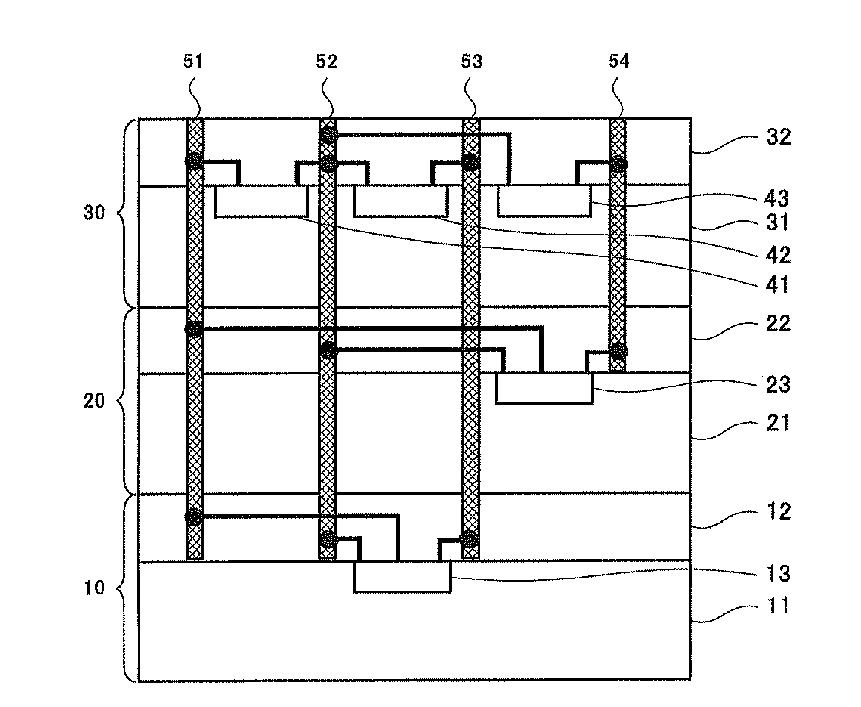
[0027]FIG. 1 is a schematic view for explaining an internal structure of a semiconductor device according to the embodiment of the invention. The semiconductor device according to the embodiment includes external terminals VDD, VSS, Pin1, and Pin2 as well as elements shown in FIG. 1.

[0028]This semiconductor device 1 according to the embodiment includes a plurality of semiconductor substrates. FIG. 1 shows a structure in which semiconductor substrates 10, 20, and 30 are layered.

[0029]The semiconductor substrate 10 includes a semiconductor layer 11 and a wiring layer 12. The semiconductor layer 11 is a layer on which a circuit element such as a transistor is formed and is made of a semiconductor...


PUM


Abstract

A semiconductor device includes: a plurality of external terminals; a plurality of semiconductor substrates that are layered; a through electrode penetrating through at least one of the semiconductor substrates and electrically connected with any of the external terminals; and a plurality of electrostatic discharge protection circuits provided on any one of the semiconductor substrates. In the device, the through electrode is electrically connected with the plurality of electrostatic discharge protection circuits.

Description

[0001]The entire disclosure of Japanese Patent Application No. 2008-306228, filed Dec. 1, 2008 is expressly incorporated by reference herein.BACKGROUND[0002]1. Technical Field[0003]The present invention relates to a semiconductor device and a method for manufacturing a semiconductor device.[0004]2. Related Art[0005]As an electronic apparatus is downsized, a mounting space for an electronic component such as a semiconductor device which is mounted inside the electronic apparatus is decreased. Therefore, electronic components such as a semiconductor device are required to be further limited.[0006]As a method for downsizing a semiconductor device, a method in which a semiconductor device is structured by layering semiconductor substrates (semiconductor chips) is proposed. In this method, semiconductor chips having the same functions as each other or semiconductor chips having different functions from each other are layered and wiring-connected with each other so as to achieve high dens...

Claims


Application Information

Patent Timeline
Patent Type & Authority Applications(United States)
IPC IPC(8): H01L23/60H01L21/60
CPCH01L23/481H01L23/60H01L2924/0002H01L2224/0401H01L2924/1815H01L24/29H01L24/32H01L24/48H01L25/0657H01L25/18H01L27/0251H01L2224/0557H01L2224/16H01L2224/48091H01L2224/48227H01L2225/0651H01L2225/06513H01L2225/06541H01L2924/078H01L2924/15311H01L2924/00014H01L2224/05552H01L2924/181H01L2924/00012H01L2224/45099H01L2224/45015H01L2924/207
Inventor SAIKI, TAKAYUKISATO, SHINYATAKAMIYA, HIROYUKI
Owner SEIKO EPSON CORP
Why Eureka
Try Eureka