Production method for semiconductor device

a production method and semiconductor technology, applied in the direction of semiconductor devices, basic electric elements, electrical appliances, etc., can solve the problems of difficult to accurately form a marking-off line in the form of a polygonal line or a curve, loss of triangular areas, and inability to effect polygonal machining or curved machining. , to achieve the effect of excellent light extraction efficiency, low cost and good area efficiency

Active Publication Date: 2007-06-28
TOYODA GOSEI CO LTD
View PDF1 Cites 22 Cited by
  • Summary
  • Abstract
  • Description
  • Claims
  • Application Information

AI Technical Summary

Benefits of technology

[0037] The present invention makes it possible to obtain a semiconductor light-emitting device having a chip form which is pentagonal or more highly polygonal and, particularly, a group III nitride semiconductor light-emitting device featuring excellent light extraction efficiency on the end surfaces of the chip and maintaining a good area efficiency over the whole semiconductor wafer surfaces at a low cost.

Problems solved by technology

The diamond blade of the dicing saw is usually in the shape of a disk which is dedicated to linear machining, and is not capable of effecting polygonal machining or curved machining.
Even a method of forming a marking-off line on the Group III nitride semiconductor layer or on a sapphire substrate, by a dicing saw with a diamond blade, is substantially linear machining because the work to be machined has a hardness comparable to the hardness of the machining material, and it is difficult to accurately form a marking-off line in the form of a polygonal line or in the form of a curve.
However, this patent document is quite silent about the method of producing the hexagonal chip.
According to this method, however, the areas of the triangular shape are lost, and the area efficiency becomes poor.
According to the conventional method of machining the polygonal chip, however, a problem remains in regard to a large machining loss and a poor area efficiency.
In many cases, however, the shape of warping varies as the machining by laser proceeds, and a machining precision is not obtained for forming separation grooves of the order of microns in the whole surface of the substrate.

Method used


Image

  • Production method for semiconductor device
  • Production method for semiconductor device
  • Production method for semiconductor device

Examples


example 1

[0082] A blue light-emitting device comprising a Group III nitride semiconductor having an orthohexagonal chip form was fabricated in a manner as described below. FIG. 5 is a plan view of a light-emitting device fabricated in this example, wherein reference numeral 1 denotes a p-electrode, 2 a p-electrode bonding pad, 3 denotes an n-type exposed surface and reference numeral 4 denotes an n-electrode.

[0083] A Group III nitride semiconductor stacked layer structure was formed by successively stacking, on a sapphire substrate having a diameter of 5.1 cm (2 inches) and a thickness of 420 μm and via a buffer layer of AlN, an underlying layer of undoped GaN having a thickness of about 4 μm, an n-side contact layer of Ge-doped (concentration of 1×10¹⁹ / cm3) GaN having a thickness of about 2 μm, an n-side clad layer of Si-doped (concentration of about 1×10¹⁸ / cm3) Ino.1Gao.9N having a thickness of about 12.5 nm, a light-emitting layer of a multiple quantum well structure, in which a barrier ...

example 2

[0090] A blue light-emitting device comprising a Group III nitride semiconductor was fabricated in a manner as described below. The form thereof on a plane was the same as that of Example 1.

[0091] A Group III nitride semiconductor stacked layer structure was formed by successively stacking, on a sapphire substrate having a diameter of 5.1 cm (2 inches) via a buffer layer of AlN, an underlying layer of undoped GaN having a thickness of about 4 μm, an n-side contact layer of Ge-doped (concentration of 1×10¹⁹ / cm3) GaN having a thickness of about 2 μm, an n-side clad layer of Ge-doped (concentration of about 1×10¹⁸ / cm3) Ino.1Gao.9N having a thickness of about 12.5 nm, a light-emitting layer of a multiple quantum well structure, in which a barrier layer of GaN having a thickness of about 16 nm and a well layer of In0-2Ga0-8N having a thickness of about 2.5 nm were stacked five times alternately and finally the barrier layer was further stacked, a p-side clad layer of Mg-doped (concentra...

example 3

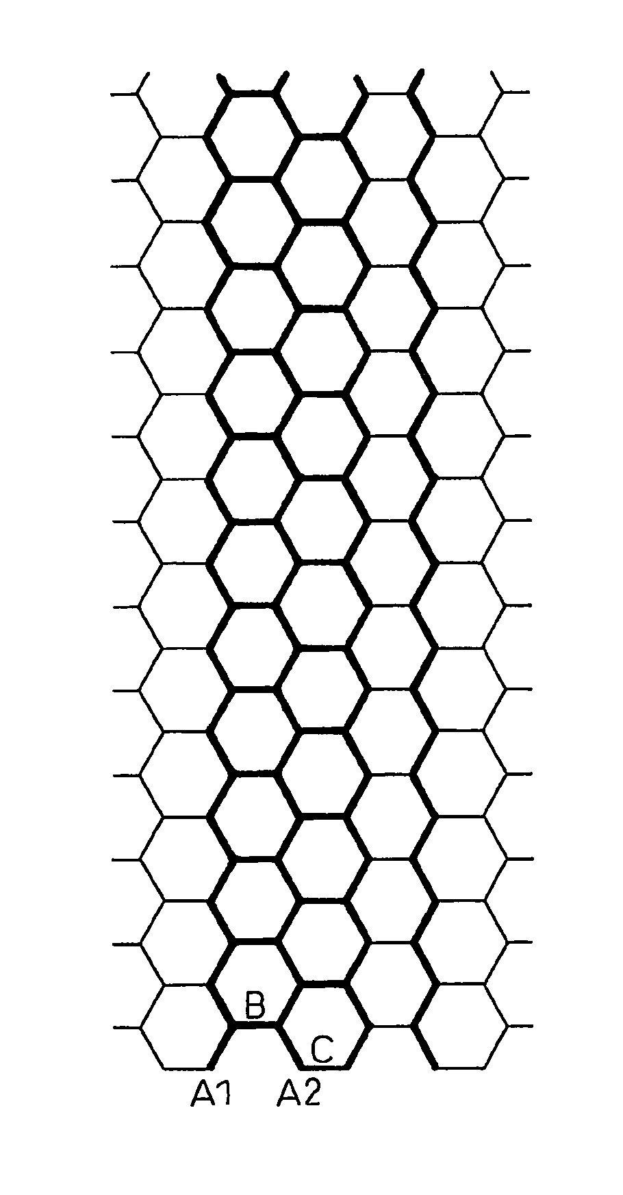
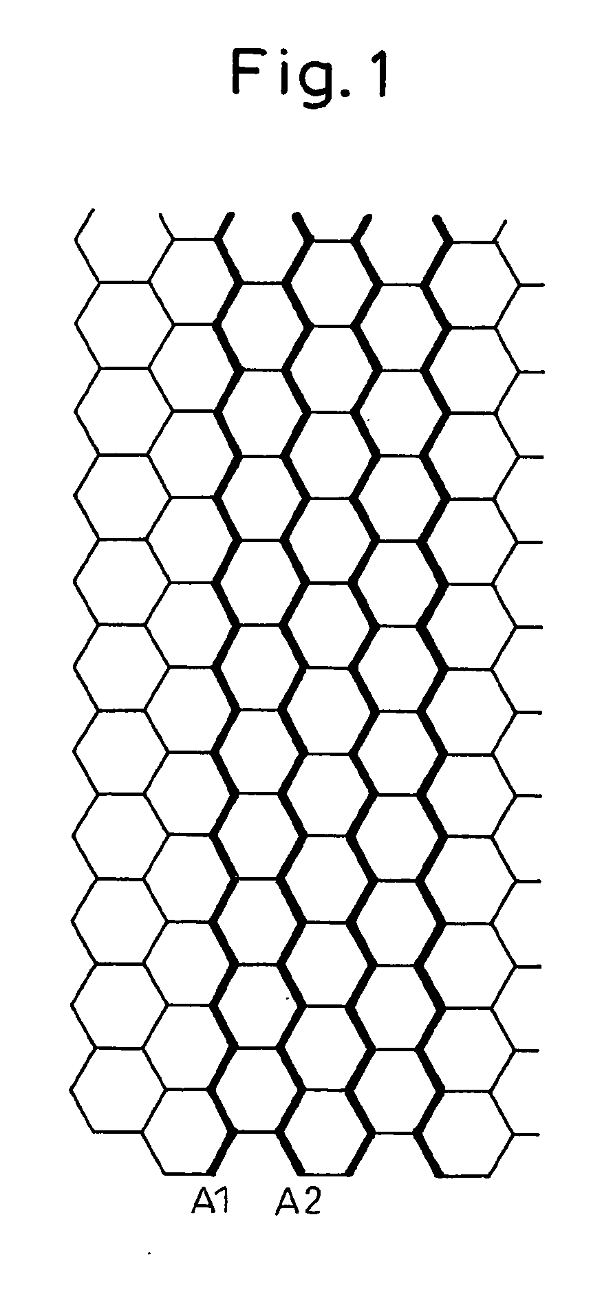
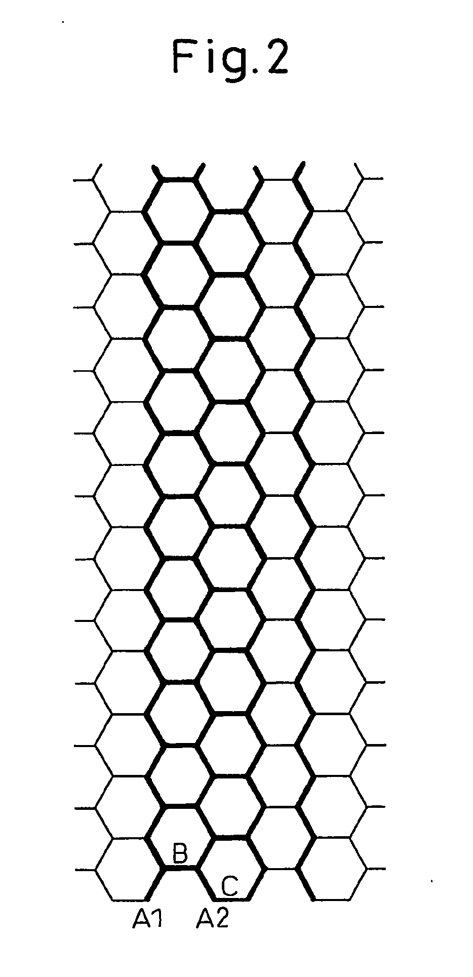
[0098] In Example 1, the laser beam was irradiated in a manner as described below. Referring to FIG. 4, separation grooves of the same length as the length of a side of a hexagonal chip form were discretely formed like a broken line in a first direction to form separation grooves (E) of the form of a broken line in the first direction. Next, the stage was turned by 60 degrees. Separation grooves of the same length as the length of the side of the hexagonal chip form were formed like a broken line starting from the ends of the separation grooves (E) of the form of a broken line in the first direction, thereby to form separation grooves (F) of the form of a broken line in a second direction. Next, the stage was turned by another 60 degrees. Separation grooves of the same length as the length of the side of the hexagonal chip form were formed like a broken line starting from the ends of the separation grooves (F) of the form of a broken line in the second direction, thereby to form sep...


PUM

PropertyMeasurementUnit
angleaaaaaaaaaa
thicknessaaaaaaaaaa
thicknessaaaaaaaaaa

Abstract

An object of the present invention is to provide a method of producing a Group III nitride semiconductor device having a chip form which is pentagonal or more highly polygonal maintaining good area efficiency and at a low cost. The inventive method of producing a Group III nitride semiconductor device having a chip shape which is a pentagonal or more highly polygonal shape comprises a first step of epitaxially growing a Group III nitride semiconductor on a substrate to form a semiconductor wafer; a second step of irradiating said semiconductor wafer with a laser beam to form separation grooves; a third step of grinding and/or polishing the main surface side differently from the epitaxially grown main surface of the substrate; and a fourth step of division into individual chips by applying stress to said separation grooves.

Description

CROSS REFERENCE TO RELATED APPLICATION [0001] This application is an application filed under 35 U.S.C. §111 (a) claiming benefit, pursuant to 35 U.S.C. §119 (e) (1), of the filing date of the Provisional Application No. 60 / 618,583 filed on Oct. 15, 2004, pursuant to 35 U.S.C. §111 (b).TECHNICAL FIELD [0002] The present invention relates to a method of producing a semiconductor device. More specifically, the invention relates to a method of producing a semiconductor chip having a pentagonal or more highly polygonal chip form (hereinafter referred to as “polygonal chip”) BACKGROUND ART [0003] A step of producing semiconductor devices by cutting a Group III nitride semiconductor wafer having an n-type layer, an active layer and a p-type layer stacked on an insulating substrate such as sapphire into chips, includes a step of forming separation grooves in a chip form by exposing the n-type layer to etching, a step of polishing the substrate to decrease its thickness, a step of exposing t...

Claims


Application Information

Patent Timeline
Patent Type & Authority Applications(United States)
IPC IPC(8): H01L21/00H01L33/00H01L33/20
CPCH01L21/0237H01L21/0242H01L21/0254H01L21/02576H01L21/02579H01L21/0262H01L21/78H01L33/0095H01L33/20
Inventor YAKUSHIJI, KENJIKUSUNOKI, KATSUKIMIKI, HISAYUKI
Owner TOYODA GOSEI CO LTD
Why Eureka
Try Eureka