Input/output interface circuit for wide I/O power supply voltage range

A technology of input and output interface and power supply voltage, applied in the direction of logic circuit coupling/interface, logic circuit connection/interface layout, logic circuit, etc. using field effect transistors, can solve problems such as leakage, application restrictions, and power loss, and achieve Wide application range, good reliability and low power consumption

Active Publication Date: 2017-06-09
VERISILICON MICROELECTRONICS SHANGHAI +3
View PDF4 Cites 9 Cited by
  • Summary
  • Abstract
  • Description
  • Claims
  • Application Information

AI Technical Summary

Problems solved by technology

However, for the existing I / O interface circuit, the I / O interface circuit designed with the function of input voltage tolerance (such as 5V input voltage tolerance) can only be used when the I / O power supply voltage is relatively high (such as 3.3 V), the input buffer stage of the I / O interface circuit can work normally
And when the I / O power supply voltage is less than 3.3V (for example, 1.8V), the input buffer stage of the existing I / O interface circuit cannot work normally
The reason is that some transistors that constitute the input buffer stage require a certain voltage for their own conduction, resulting in a certain voltage drop in the input voltage of the I / OPAD terminal, which makes the input buffer stage unable to drive and transmit the input signal of the off-chip device to the inside of the chip.
As a result, the existing I / O interface circuit can only work in a relatively narrow I / O power supply voltage range, its application is limited, and it cannot meet the needs of a wide variety of off-chip devices with different interface standards
In addition, in the output buffer stage of some existing I / O interface circuits, when the input voltage of the I / O PAD terminal is equal to 5V (input voltage tolerance), leakage often occurs in the circuit, resulting in unnecessary power consumption loss

Method used


Image

  • Input/output interface circuit for wide I/O power supply voltage range
  • Input/output interface circuit for wide I/O power supply voltage range
  • Input/output interface circuit for wide I/O power supply voltage range

Examples


Embodiment Construction

[0057] The following describes the implementation of the present invention through specific specific examples. Those skilled in the art can easily understand other advantages and effects of the present invention from the content disclosed in this specification. The present invention can also be implemented or applied through other different specific embodiments, and various details in this specification can also be modified or changed based on different viewpoints and applications without departing from the spirit of the present invention.

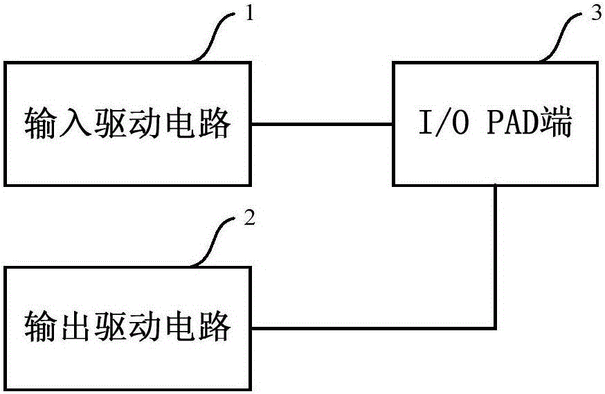
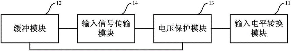
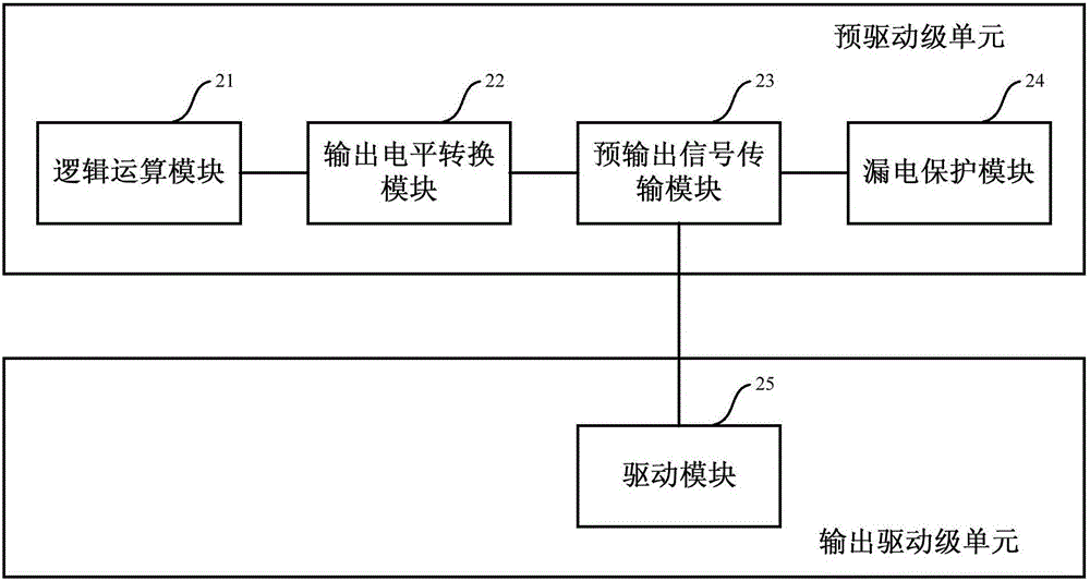
[0058] See figure 1 with figure 2 The first embodiment of the present invention relates to an input / output interface circuit for a wide I / O power supply voltage range. It should be noted that the illustrations provided in this embodiment mode only illustrate the basic idea of ​​the present invention in a schematic manner. The figures only show the components related to the present invention instead of the number, shape, and shape of the compo...


PUM


Abstract

The invention provides an input/output interface circuit for a wide I/O power supply voltage range; the input/output interface circuit at least comprises the following units: an I/O PAD end; an input drive circuit used for transmitting an off-chip device input signal of the I/O PAD end to the inner side chip; an output drive circuit used for transmitting a chip inner output signal to the off-chip device through the I/O PAD end. When the I/O PAD end input voltage is the I/O power supply voltage or higher than the I/O power supply voltage tolerance voltage, the input/output interface circuit can use the input drive circuit and/or output drive circuit to realize normal signal transmission without electric leakage, thus allowing the I/O power supply voltage of the input/output interface circuit to be within the wide I/O power supply voltage range. The input/output interface circuit can work in the wide I/O power supply voltage range, and can work under a condition in which the I/O PAD end input voltage is higher than the I/O power supply voltage tolerance voltage.

Description

Technical field [0001] The invention relates to the technical field of large-scale integrated circuit design, and is suitable for SOC (System On Chip, system on chip), and particularly relates to an input and output interface circuit used for a wide I / O power supply voltage range. Background technique [0002] The integrated circuit chip is connected with the outside world through the input and output interface (Input / Output interface). The I / O interface receives the input signal of the off-chip device and transmits it to the chip, and can also receive the internal output signal of the chip to drive the off-chip device . In integrated circuits, signals are generally connected to the outside world through input and output buffer stages and I / O PAD (I / O pressure solder joints). The function of input and output buffer stages is to match on-chip signals with off-chip signals. [0003] Due to the wide variety of off-chip devices and different interface standards, the I / O interface circ...

Claims


Application Information

Patent Timeline
Patent Type & Authority Applications(China)
IPC IPC(8): H03K19/0185H03K19/003
CPCH03K19/00315H03K19/018507
Inventor 邹峰费伟斌肖艳周柏毓
Owner VERISILICON MICROELECTRONICS SHANGHAI
Why Eureka
Try Eureka