Exposure method for large-sized spliced product

An exposure method and large-scale technology, applied in the field of integrated circuit manufacturing, can solve the problem of high cost of photomasks, achieve the effects of reduced work intensity, good overlay accuracy and splicing alignment accuracy, and cost savings of photomasks

Active Publication Date: 2017-06-13
SHANGHAI HUALI MICROELECTRONICS CORP
View PDF4 Cites 4 Cited by
  • Summary
  • Abstract
  • Description
  • Claims
  • Application Information

AI Technical Summary

Problems solved by technology

This method has two defects: (1) Different masks are required to expose different areas, and the cost of multiple masks is high; (2) The exposure model can only choose ASML lithography machine

Method used


Image

  • Exposure method for large-sized spliced product
  • Exposure method for large-sized spliced product
  • Exposure method for large-sized spliced product

Examples


Embodiment Construction

[0029] In order to make the purpose, technical solution and advantages of the present invention clearer, the specific implementation manners of the present invention will be further described in detail below in conjunction with the accompanying drawings.

[0030] A method for exposing large-scale spliced ​​products, comprising the following steps:

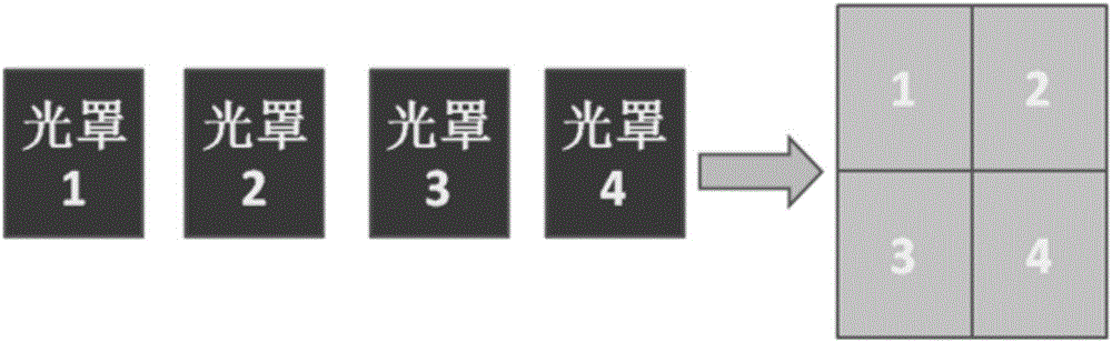
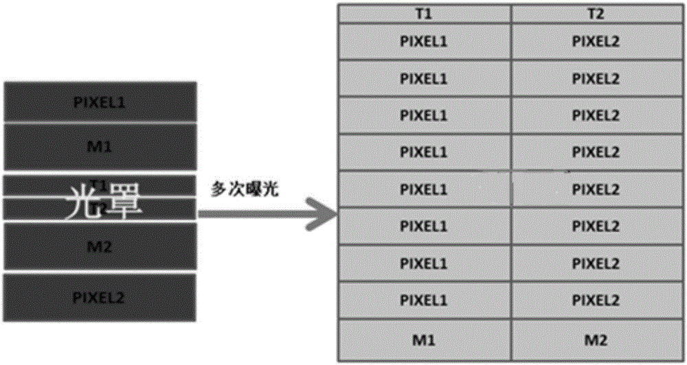
[0031] S1: Divide the rectangular mask into six areas from top to bottom, which are PIXEL1 area, M1 area, T1 area, T2 area, M2 area and PIXEL2 area from top to bottom. The lengths of the six areas are equal to the length of the mask. width with a blackout band between each area.

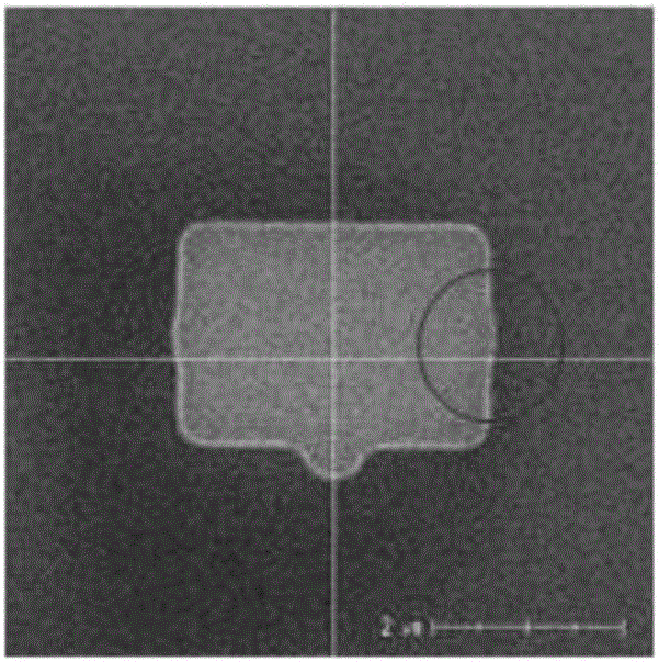
[0032] The size of each area in the photomask is smaller than the maximum exposure size of the photolithography machine, the size of the entire photomask is larger than the maximum exposure size of the photolithography machine, and the M1 area, T1 area, T2 area and M2 area are all placed with overlay alignment marks, Used to monitor in-wafer overlay accu...


PUM


Abstract

The invention discloses an exposure method for a large-sized spliced product. The exposure method comprises the following steps: dividing a photomask into six areas; selecting a functional part and a nonfunctional part from a wafer, wherein the functional part is formed by splicing and exposing complete functional units, and the nonfunctional part is formed by splicing and exposing incomplete functional units; splicing and exposing the complete functional units; splicing and exposing the incomplete functional units; completely splicing and exposing the functional part and the nonfunctional part in the wafer, wherein the incomplete functional units and the complete functional units are the same in size, but the exposure times of the incomplete functional units are far less than the exposure times of the complete functional units. The exposure method for the large-sized spliced product, provided by the invention, has good properties of reducing the exposure times, improving alignment precision and splicing alignment, and avoiding a sun-shading belt from forming a long line.

Description

technical field [0001] The invention relates to the field of integrated circuit manufacturing, in particular to an exposure method for large-size splicing products. Background technique [0002] With the development of digital technology and semiconductor manufacturing technology, image sensors, as optoelectronic components in the optoelectronic industry, can be described as changing with each passing day. Some professional imaging applications such as astronomical telescopes, full-frame digital cameras, and medical imaging require large-size image sensors. Since these large-size image sensors have exceeded the image field of the lithography machine, the maximum size of a single exposure is 26*33 mm, so splicing technology needs to be used in the manufacturing process. Splicing technology, as the name implies, is to partition the involved graphics in the mask during the chip manufacturing process, select the corresponding areas in the complete functional unit (shot) and exp...

Claims


Application Information

Patent Timeline
Patent Type & Authority Applications(China)
IPC IPC(8): G03F7/20G03F7/22
CPCG03F7/2022G03F7/22G03F7/70475
Inventor 李飞吴鹏郑海昌
Owner SHANGHAI HUALI MICROELECTRONICS CORP
Why Eureka
Try Eureka