LED device packaging method and LED device

A technology of LED devices and packaging methods, applied in semiconductor devices, electrical components, circuits, etc., can solve the problems of glue failure, difficult process, and difficult molding, etc., and achieve the effect of low cost and simple production process

Inactive Publication Date: 2017-06-13
光创空间(深圳)技术有限公司
View PDF2 Cites 39 Cited by
  • Summary
  • Abstract
  • Description
  • Claims
  • Application Information

AI Technical Summary

Problems solved by technology

Although this method can prolong the service life, long-term exposure will still cause the glue to fail, making the LED device airtight not good, and even the cover plate will fall off.
This kind of ceramic bracket with steps is difficult to form, the welding effect is poor, and the process is difficult
All in all,...

Method used


Image

  • LED device packaging method and LED device
  • LED device packaging method and LED device
  • LED device packaging method and LED device

Examples


Embodiment Construction

[0018] The concept, specific structure and technical effects of the present invention will be clearly and completely described below in conjunction with the embodiments and accompanying drawings, so as to fully understand the purpose, features and effects of the present invention. Apparently, the described specific embodiments are only some embodiments of the present invention, not all embodiments. Based on the embodiments of the present invention, other embodiments obtained by those skilled in the art without paying creative efforts are all Belong to the protection scope of the present invention. The various technical features in the invention can be combined interactively on the premise of not contradicting each other.

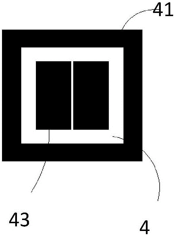
[0019] The embodiment of the present invention is achieved as follows: an inorganic packaged LED device, first sputtering a layer of metal copper on the front and back of the planar ceramic substrate to form a metal layer 41 and a metal layer 42; wherein the...


PUM

PropertyMeasurementUnit
Thicknessaaaaaaaaaa
Thicknessaaaaaaaaaa
Thicknessaaaaaaaaaa

Abstract

The invention belongs to the field of semiconductor packaging, and is especially suitable for the packaging of light source devices with high luminous flux density, short wavelength and high energy output, such as semiconductor light emitting devices (LEDs) and laser lighting packaging devices. It relates to a packaging method for an LED device. The LED device is composed of a transparent inorganic sealing cover plate, a metal sealing ring, a ceramic substrate, an LED chip, and LED welding wires. Through the transparent inorganic sealing cover plate, the metal sealing ring and the The ceramic substrate is eutectically welded for packaging to form a hermetic LED device.

Description

technical field [0001] The invention belongs to the field of semiconductor packaging, and is especially suitable for the packaging of light source devices with high luminous flux density and short wavelength and high energy output, such as semiconductor light emitting devices (LEDs) and laser lighting packaging devices, and relates to a method for packaging LED devices and LED devices. device. Background technique [0002] At present, in the field of LED packaging, organic glue is mainly used to package LED chips. Some LEDs are potted with organic glue in the reflective cavity of the bracket, and some LED chips are covered with organic glue in various shapes by mold molding technology. The light emitted by the LED chip is transmitted through the organic glue. When the light emitted by the LED chip has a high energy density, the molecular chain of the organic glue will break after a long time of irradiation, resulting in color changes such as yellowing, and the glue itself w...

Claims


Application Information

Patent Timeline
IPC IPC(8): H01L33/52H01L33/62
CPCH01L33/52H01L33/62
Inventor 邓玉仓石维志耿占峰
Owner 光创空间(深圳)技术有限公司
Why Eureka
Try Eureka