Supercharge Your Innovation With Domain-Expert AI Agents!

Printed circuit board perforating device

A technology for printed circuit boards and punching devices, which is applied in the directions of printed circuits, printed circuit manufacturing, electrical components, etc., can solve problems such as inability to clean the holes and slag, and achieve the effect of saving processing time and facilitating storage.

Active Publication Date: 2017-06-13
SUZHOU FUTENG INTELLIGENT TECH CO LTD
View PDF6 Cites 0 Cited by
  • Summary
  • Abstract
  • Description
  • Claims
  • Application Information

AI Technical Summary

Problems solved by technology

[0008] The present invention intends to provide a printed circuit board punching device to solve the problem that the existing punching device cannot clean the hole slag when punching

Method used


Image

  • Printed circuit board perforating device

Examples


Embodiment Construction

[0032] The present invention will be described in further detail below by means of specific embodiments:

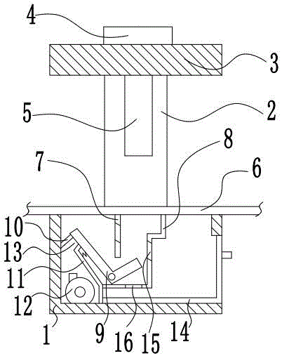
[0033] The reference signs in the drawings of the description include: support base 1, vertical arm 2, cross arm 3, motor 4, drill bit 5, PCB board 6, left side board 7, right side board 8, swing rod 9, slant board 10, Z-shaped plate 11, blower 12, air outlet 13, drawer 14, return air hole 15, leakage hole 16.

[0034] like figure 1 As shown, the printed circuit board punching device includes a support base 1 at the bottom and a suspension arm installed on the support base 1 . The suspension arm includes a vertical arm 2 perpendicular to the support base 1 and a cross arm 3 vertically connected to the top of the vertical arm 2 . The cross arm 3 is equipped with a motor 4 and a drill bit 5 connected with the motor 4 and passing through the cross arm 3 to extend downwards for punching a PCB board 6 . The support base 1 is a hollow structure with an upper end opening, and...


PUM


Abstract

The invention discloses a printed circuit board perforating device. The perforating device comprises a supporting base, a suspension arm arranged on the supporting base, a motor arranged on the suspension arm and a drill bit connected with the motor to extend downwardly for PCB plate perforation; the supporting base is of hollow structure with an open upper end, a left side plate used for supporting the PCB plate and a right side plate which is stair-stepping are arranged in the supporting base, a blanking channel located below the drill bit is formed by the left side plate and the right side plate to allow blanking on the PCB plate to pass through, the right side plate is provided with a first ladder portion and a second ladder portion which extend to the left successively, the extension end of the second ladder portion is connected with a Z-shaped plate connected with the underside of the supporting base, the left side of the supporting base is provided with a sloping plate inclining to the upper right, a ventilation cavity is formed by the sloping plate, the Z-shaped plate and the supporting base, and is provided with a blower, an air outlet is formed by the sloping plate and the Z-shaped plate to blow up the PCB plate, a V-shaped oscillating bar is arranged between the second ladder portion of the left side plate and the right side plate.

Description

technical field [0001] The invention relates to the field of printed circuit board processing, in particular to a printed circuit board punching device and a method for using the same. Background technique [0002] Printed circuit board, also known as PCB (Printed Circuit Board) board, is an important electronic component, a support for electronic components, and a provider of electrical connections for electronic components. [0003] During the production process of the PCB board, it needs to be drilled. Some of the drilled holes are used to make via holes for copper plating of various layers of circuits, and some are used to make positioning holes. [0004] After the PCB board is mechanically drilled, some copper wire and PP dust will accumulate in the hole when the PCB board hole is formed, forming hole slag. The hole slag is mainly copper foil, copper wire, glass fiber, PP powder and other dust. It leaves great quality hidden dangers for the subsequent electroplating pr...

Claims


Application Information

Patent Timeline
Patent Type & Authority Applications(China)
IPC IPC(8): H05K3/00B26F1/16
CPCB26F1/16H05K3/00H05K3/0047
Inventor 周建勋
Owner SUZHOU FUTENG INTELLIGENT TECH CO LTD
Features
  • R&D
  • Intellectual Property
  • Life Sciences
  • Materials
  • Tech Scout
  • Unparalleled Data Quality
  • Higher Quality Content
  • 60% Fewer Hallucinations
Learn More