Inductor structure and its formation method
A technology of inductance and electrical connection, applied in the field of inductance, can solve problems affecting the performance of integrated circuits, etc., and achieve the effects of enhancement and reduction, suppression of interactive noise, and increase in density
- Summary
- Abstract
- Description
- Claims
- Application Information
AI Technical Summary
Problems solved by technology
Method used
Image

Examples
Embodiment Construction
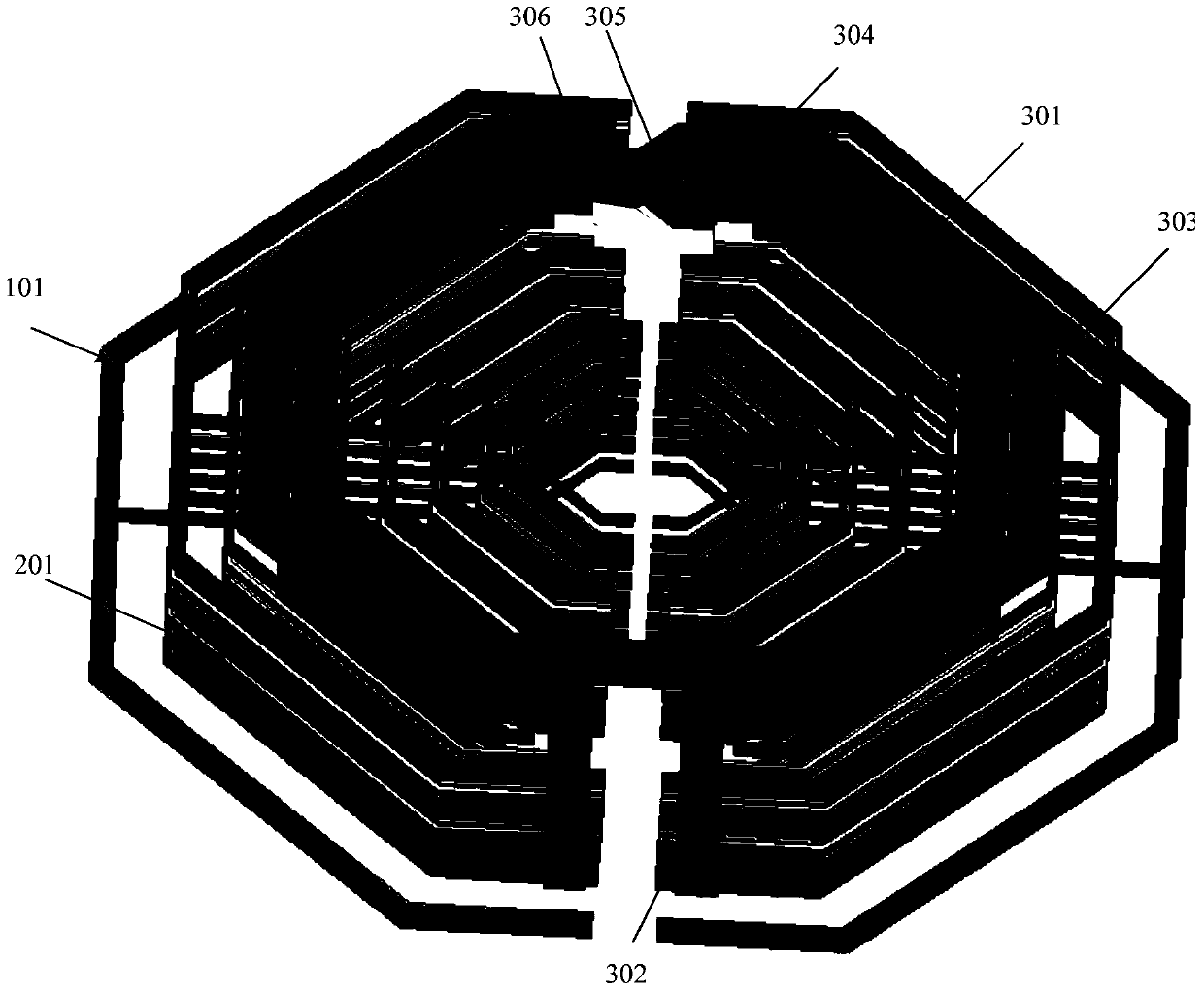
[0032] Cross talk noise is likely to be generated between the inductor fabricated by the existing integration process and the substrate or with other devices, which affects the performance of the integrated circuit.
[0033] The study found that the reason for the generation of cross talk noise is: there will be coupling capacitance and coupling inductance between the inductor and the substrate or between the inductor and other devices. Affects the performance of other devices and affects the quality factor of the inductor.
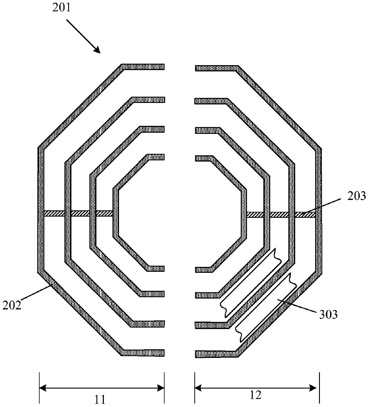
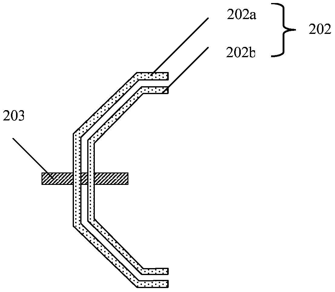
[0034] To this end, the present invention provides an inductance structure. There are several stacked metal shielding layers between the inductance layer and the ground terminal of the substrate, the upper and lower metal shielding layers are electrically connected to each other, and the bottom metal shielding layer is electrically connected to the ground terminal. , each metal shielding layer includes a first part and a second part that are disconnected ...
PUM
 Abstract
Description
Claims
Application Information
 - R&D
- Intellectual Property
- Life Sciences
- Materials
- Tech Scout
- Unparalleled Data Quality
- Higher Quality Content
- 60% Fewer Hallucinations
Browse by: Latest US Patents, China's latest patents, Technical Efficacy Thesaurus, Application Domain, Technology Topic, Popular Technical Reports.
© 2025 PatSnap. All rights reserved.Legal|Privacy policy|Modern Slavery Act Transparency Statement|Sitemap|About US| Contact US: help@patsnap.com