Manufacture method of storage component

A manufacturing method and storage element technology, which is applied in semiconductor/solid-state device manufacturing, electrical components, semiconductor devices, etc., can solve problems such as resistance increase, reading and writing time failure, and contact area reduction, so as to improve the contact area reduction and reduction Process cost, effect of simplifying process steps

Active Publication Date: 2017-06-20
WINBOND ELECTRONICS CORP
View PDF4 Cites 15 Cited by
  • Summary
  • Abstract
  • Description
  • Claims
  • Application Information

AI Technical Summary

Problems solved by technology

However, in the prior art, multiple photolithography processes are used to separately form the isolation structure and the contact window of the capacitor, which is prone to alignment problems.
The alignment problem becomes more and more serious as the size of the device shrinks, for example, it tends to reduce the contact area between the active region (such as the source / drain region) and the contact window of the capacitor.
As the contact area between the active area and the capacitor contact window becomes smaller, the resistance between the active area and the capacitor contact window will increase, which will lead to the failure of the read and write time

Method used


Image

  • Manufacture method of storage component
  • Manufacture method of storage component
  • Manufacture method of storage component

Examples


Embodiment Construction

[0044] The present invention will be described more fully with reference to the accompanying drawings of this embodiment. However, the present invention can also be embodied in various forms and should not be limited to the embodiments described herein. In the drawings, the thicknesses of layers and regions may be exaggerated for clarity. The same or similar reference numbers represent the same or similar components, and the following paragraphs will not repeat them one by one.

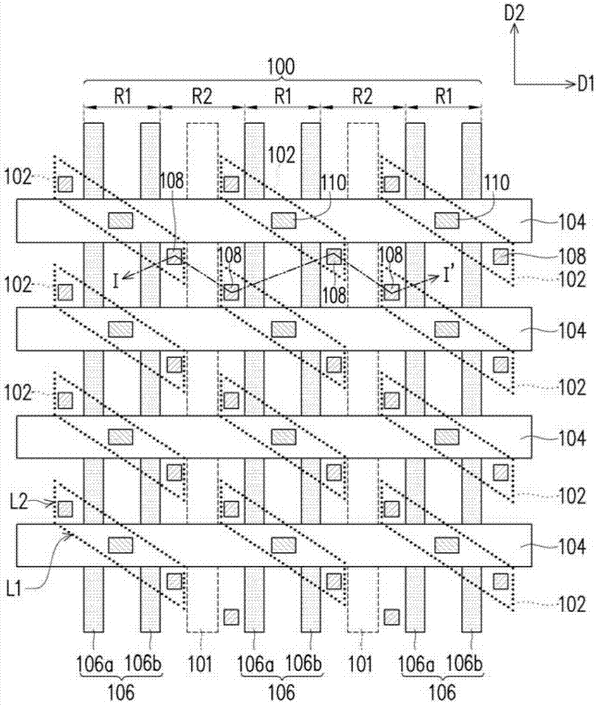
[0045] figure 1 is a schematic top view of the storage element of the first embodiment of the present invention.

[0046] Please refer to figure 1 , the present embodiment provides a storage element comprising: a substrate 100, a plurality of isolation structures 101, a plurality of active regions 102, a plurality of bit lines 104, a plurality of word line groups 106, a plurality of capacitor contact windows 108 and a plurality of The bit line contacts the window 110 . For clarity of the figure, ...


PUM


Abstract

The invention provides a manufacture method of a storage component, wherein the manufacture method comprises supplying a substrate with a first region and a second region; forming a first dielectric layer on the first region of the substrate; forming a conductor layer on the second region of the substrate, wherein the top layer of the conductor layer is lower than that of the first dielectric layer; forming a second dielectric layer on the substrate; removing partial second dielectric layer and partial conductor layer, thereby forming first openings in the conductor layer and the second dielectric layer of the second region, wherein the first openings are exposed on the surface of the substrate; removing the substrate on the partial second region, thereby forming a groove in the substrate of the second region; and forming a third dielectric layer in the groove in the first opening. The manufacture method of the storage component can reduce process steps for reducing process cost.

Description

technical field [0001] The invention relates to a manufacturing method of a semiconductor component, in particular to a manufacturing method of a storage element. Background technique [0002] In order to improve the integration of dynamic random access memory to speed up the operation speed of components, and to meet the needs of consumers for miniaturized electronic devices, a buried word line dynamic random access memory (buried word line DRAM) has been developed in recent years. to meet the above-mentioned needs. However, as the memory density increases, the word line spacing and the isolation structure of the memory array will continue to shrink, resulting in various adverse effects. For example, leakage between memory (Cell-to-cell leakage), interference between word lines (also known as RowHammer), read and write time failure (t WR failure), retention failure, bit line coupling failure (Bit Line coupling failure), etc. [0003] Therefore, in order to address the i...

Claims


Application Information

Patent Timeline
Patent Type & Authority Applications(China)
IPC IPC(8): H01L21/762
CPCH01L21/762H01L21/76224H10B12/0335H10B12/09H10B12/50
Inventor 简毅豪田中义典张维哲
Owner WINBOND ELECTRONICS CORP
Why Eureka
Try Eureka