Chip embedded silicon substrate type fan-out type packaging structure and manufacturing method therefor

A packaging structure, fan-out technology, applied in semiconductor/solid-state device manufacturing, electrical components, electric solid-state devices, etc., can solve silicon substrate etching cost and process difficulty, etching silicon substrate uniformity difficulty, crystal Large round warpage and other problems, to achieve the effect of reducing etching and packaging costs, reducing packaging costs, and reducing warpage

Active Publication Date: 2017-06-20
HUATIAN TECH KUNSHAN ELECTRONICS
View PDF7 Cites 19 Cited by
  • Summary
  • Abstract
  • Description
  • Claims
  • Application Information

AI Technical Summary

Problems solved by technology

[0002] Fan-out wafer-level packaging technology currently uses a silicon base instead of a plastic encapsulant, and uses a silicon base instead of a molding compound as the fan-out base. , can accurately etch structures such as holes and grooves, and has good heat dissipation performance, but there are also certain shortcomings. In this way, the chip can be completely placed in the deep groove. However, when the silicon substrate is etched deeply, it is difficult to ensure the uniformity of the silicon substrate, and the etching cost and process of the silicon substrate are difficult. , the wafer warpage is also large

Method used


Image

  • Chip embedded silicon substrate type fan-out type packaging structure and manufacturing method therefor
  • Chip embedded silicon substrate type fan-out type packaging structure and manufacturing method therefor
  • Chip embedded silicon substrate type fan-out type packaging structure and manufacturing method therefor

Examples


Embodiment 1

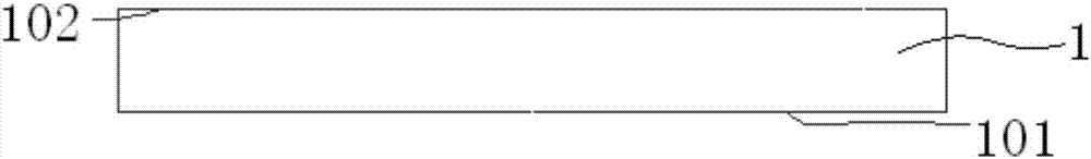
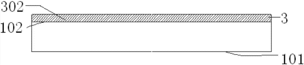
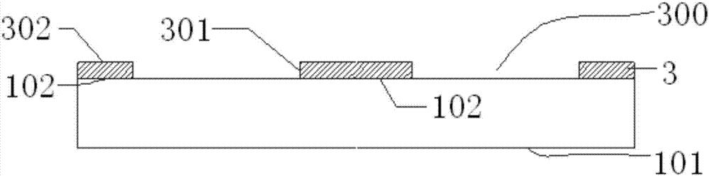
[0052] Such as Figure 1.1-Figure 1.10 Shown is a cross-sectional view of a chip-embedded fan-out package structure according to an embodiment of the present invention. The packaging structure in this embodiment 1 includes a silicon substrate 1, the silicon substrate 1 has a first surface 102 and a second surface 101 opposite to it, and at least one Groove A103 that two surfaces extend, and this groove A103 depth is relatively shallow, that is to say the bonding pad surface of the chip that places in it will be higher than the first surface of silicon substrate a certain distance, and this groove A is preferably straight groove or The angle between the side wall and the bottom surface is 80 to 120°. The structure diagram of this embodiment is a straight groove shape; the first surface of the silicon substrate is laid with a thick glue layer 3, that is, the thick glue layer 3 is located on the first surface of the silicon substrate. On a surface 102, the upper surface 302 of t...

Embodiment 2

[0093] Such as Figure 2.1-Figure 2.11 As shown, as shown in the cross-sectional view of a chip-embedded fan-out package structure according to another embodiment of the present invention, Embodiment 2 of the present invention basically includes the technical features of Embodiment 1, and the difference is that the thick adhesive layer is No photoresist, and the thick glue layer covers the side of the chip and fills the gap between the side of the chip and the groove A; the thick glue layer and the pad surface of the chip are laid with A dielectric layer, on which a metal wiring layer, a passivation layer, and conductive bumps are sequentially arranged, and at least part of the conductive bumps fan out above the thick adhesive layer, and the metal wiring layer passes through the dielectric layer The opening formed on the passivation layer is electrically connected to the pad of the chip, and the conductive bump is electrically connected to the metal wiring layer through the op...


PUM


Abstract

The invention discloses a chip embedded silicon substrate type fan-out type packaging structure and a manufacturing method therefor. The packaging structure comprises a silicon substrate, wherein the silicon substrate has a first surface and a second surface; at least one groove A which extends to the second surface is formed in the first surface of the silicon substrate; at least one chip with an upward bonding pad surface is arranged in the groove A; the bonding pad surface of the chip is higher than the first surface of the silicon substrate for a certain distance; a thick adhesive layer which exposes the groove A and the chip is paved on the first surface; the sum of the thickness of the thick adhesive layer and the depth of the groove A is close to or equal to the thickness of the chip; and the electric power of the bonding pad of the chip is fan out to the upward side of the thick adhesive layer through a metal wiring layer. The thick adhesive layer is introduced to the surface of the silicon substrate, and the thick adhesive layer and the silicon substrate are jointly used as a chip fan-out carrier, so that requirement on the groove etching depth and the groove bottom etching uniformity in embedding the chip in the silicon substrate can be lowered, and the purposes of shortening etching process time on the silicon substrate, lowering etching and packaging costs and reducing warping degree are achieved.

Description

technical field [0001] The invention relates to the technical field of semiconductor packaging, in particular to a chip-embedded silicon-based fan-out packaging structure and a manufacturing method thereof. Background technique [0002] Fan-out wafer-level packaging technology currently uses a silicon base instead of a plastic encapsulant, and uses a silicon base instead of a molding compound as the fan-out base. , can accurately etch structures such as holes and grooves, and has good heat dissipation performance, but there are also certain shortcomings. In this way, the chip can be completely placed in the deep groove. However, when the silicon substrate is etched deeply, it is difficult to ensure the uniformity of the silicon substrate, and the etching cost and process of the silicon substrate are difficult. , wafer warpage is also large. Contents of the invention [0003] In order to solve the above-mentioned technical problems, the present invention proposes a chip-e...

Claims


Application Information

Patent Timeline
Patent Type & Authority Applications(China)
IPC IPC(8): H01L23/488H01L23/29H01L23/373H01L21/50
CPCH01L21/50H01L23/293H01L23/3738H01L23/488H01L2224/04105H01L2224/12105H01L2224/19H01L2224/32225H01L2224/73267H01L2224/92244H01L2224/97H01L2924/15153
Inventor 于大全邹益朝黄真瑞
Owner HUATIAN TECH KUNSHAN ELECTRONICS
Why Eureka
Try Eureka