Imaging method and imaging device of image sensor and electronic device

An image sensor and imaging method technology, applied in image communication, radiation control devices, image signal generators, etc., can solve the problems of reducing image detail and non-detail contrast, image blur, image noise, etc., to improve user experience , Improve the effect of brightness

Inactive Publication Date: 2017-06-20
BYD CO LTD
View PDF4 Cites 15 Cited by
  • Summary
  • Abstract
  • Description
  • Claims
  • Application Information

AI Technical Summary

Problems solved by technology

[0004] 1) Increase the analog or digital gain, that is, multiply the image signal by a multiple greater than 1, so that the image signal can be amplified to improve the image brightness, but when the image signal is amplified, the image noise will also be enlarged by the same multiple , resulting in too much image noise after amplification;
[0005] 2) In the image processing part, adding a brightness to the image and adding a brightness to the whole image can achieve the effect of improving the low-light brightness of the image, but at the same time, increasing the brightness will reduce the contrast between image details and non-details, resulting in The image looks very blurry;
[0006] 3) The all-pass lens is adopted, which only allows visible light to pass through compared with ordinary lenses, and the all-pass lens can also pass infrared light, so that the image brightness obtained by the image sensor is higher, but the image is prone to color cast during the day

Method used


Image

  • Imaging method and imaging device of image sensor and electronic device
  • Imaging method and imaging device of image sensor and electronic device
  • Imaging method and imaging device of image sensor and electronic device

Examples


Embodiment Construction

[0024] Embodiments of the present invention are described in detail below, examples of which are shown in the drawings, wherein the same or similar reference numerals designate the same or similar elements or elements having the same or similar functions throughout. The embodiments described below by referring to the figures are exemplary and are intended to explain the present invention and should not be construed as limiting the present invention.

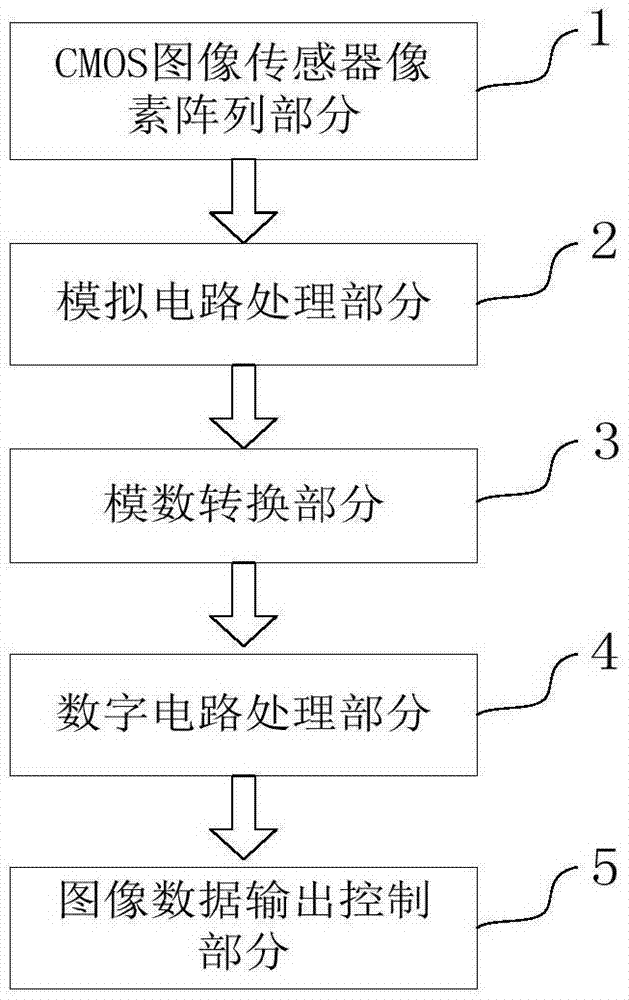
[0025] Firstly, the working process of the CMOS image sensor in the related art is introduced. Such as figure 1 As shown, step 1: the pixel array part of the image sensor converts the optical signal into an electrical signal through photoelectric induction; step 2: the electrical signal is processed by the analog circuit processing part; step 3: the analog electrical signal is converted into a digital signal by the analog-to-digital conversion part; Step 4: The digital signal is processed by the digital processing part; finally,...


PUM


Abstract

The invention discloses an imaging method and imaging device of an image sensor and an electronic device. The image sensor includes a pixel array and a micro lens array arranged on the pixel array. Each four adjacent pixels in the pixel array include a red pixel, a green pixel, a blue pixel and an infrared pixel. The micro lens array includes a plurality of micro lens. Each micro lens covers one pixel correspondingly. The imaging method includes reading output of each pixel in the pixel array; performing interpolation treatment on the output of each pixel so as to obtain a red component, a green component, a blue component and an infrared component corresponding to each pixel; acquiring the type of a current shooting scene; determining three-primary color output values of each pixel according to the type of the current shooting scene so as to output images according to the three-primary color output values of each pixel. By adopting the imaging method, image luminance during dark scene shooting is improved substantially and image color shift in non-dark scene shooting is avoided, so that user experience is improved.

Description

technical field [0001] The invention relates to the field of imaging technology, in particular to an imaging method of an image sensor, an imaging device and electronic equipment. Background technique [0002] In recent years, the development of image sensors has advanced by leaps and bounds, sales have continued to rise, and manufacturers have also sprung up. The market competition is extremely fierce. While prices continue to decline, the requirements for image quality continue to increase. In order to reduce costs and sensors. Area, the pixel size of the image sensor is getting smaller and smaller, and the smaller pixel size of the image sensor will have a great impact on the imaging quality of the sensor. One of the indicators that has the greatest impact is the low-light effect of the image sensor. The smaller the pixel The smaller the image sensor, the lower the sensitivity of the image sensor, and the less brightness of the image in low light. In order to improve the ...

Claims


Application Information

Patent Timeline
Patent Type & Authority Applications(China)
IPC IPC(8): H04N9/04
CPCH01L27/148H01L27/14609H04N23/00H04N23/11H04N25/50H04N23/843H04N25/131H04N23/84H04N25/00
Inventor 毛水江郭先清
Owner BYD CO LTD
Why Eureka
Try Eureka