Mask blank

A mask and blank technology, applied in the direction of optics, instruments, photoplate process of pattern surface, etc., can solve problems such as complex circuit patterns, and achieve the effect of minimizing image distortion and mask warping

Inactive Publication Date: 2017-06-27
TAIWAN SEMICON MFG CO LTD
View PDF0 Cites 2 Cited by
  • Summary
  • Abstract
  • Description
  • Claims
  • Application Information

AI Technical Summary

Problems solved by technology

For example, masks used in high-resolution lithography to transfer small and complex circuit patterns may present new challenges

Method used


Image

  • Mask blank
  • Mask blank
  • Mask blank

Examples


Embodiment Construction

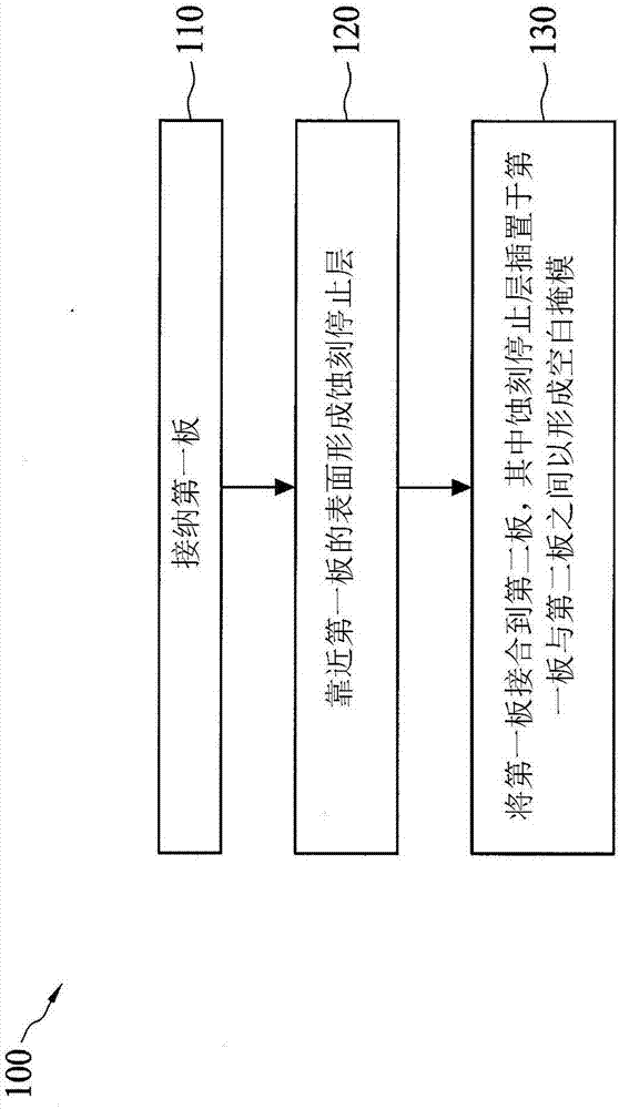
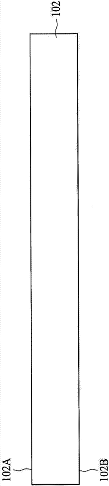
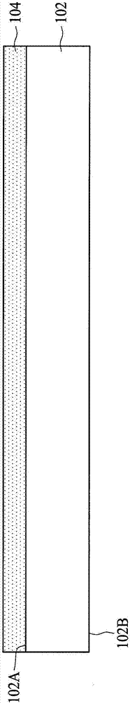
[0016] The following disclosure provides many different embodiments, or examples, of different means for implementing the provided subject matter. Specific examples of components and arrangements are described below to simplify the present disclosure. Of course, these are examples only and are not intended to be limiting. For example, in the following description, the first member is formed on or on the second member may include the embodiment that the first member and the second member are formed in direct contact, and may also include that an additional member may be formed on the first member. An embodiment in which the first member and the second member are not in direct contact between a member and the second member. In addition, the embodiments of the present invention may repeat element symbols and / or letters in various instances. This repetition is for simplicity and clarity and does not in itself dictate a relationship between the various embodiments and / or configur...


PUM


Abstract

A mask blank and a mask are provided. The mask blank includes a substrate, and an etching stop layer embedded in the substrate. The mask includes the mask blank with the embedded etching stop layer, and a plurality of recesses formed in the mask blank. The recess exposes the embedded etching stop layer.

Description

technical field [0001] Embodiments of the present invention relate to a blank mask, a mask and a manufacturing method thereof. Background technique [0002] The semiconductor integrated circuit (IC) industry has experienced exponential growth. Technological advances in IC materials and design have produced generations of ICs, each generation having smaller and more complex circuits than the previous generation. In the course of IC evolution, functional density (ie, the number of interconnected devices per chip area) has generally increased, while geometry size (ie, the smallest component or line that can be produced using a fabrication process) has decreased. [0003] This scaling down process generally provides advantages by increasing production efficiency and reducing associated costs. This scaling down also increases the complexity of handling and manufacturing the ICs. To achieve these advances, similar developments in IC processing and manufacturing are required. F...

Claims


Application Information

Patent Timeline
Patent Type & Authority Applications(China)
IPC IPC(8): G03F1/50
CPCG03F1/50G03F1/60G03F1/26G03F1/80H01L21/0338H01L21/0332H01L21/0337
Inventor 涂志强陈俊郎
Owner TAIWAN SEMICON MFG CO LTD
Why Eureka
Try Eureka