Solar cell, solar cell manufacturing method and electrical equipment

A technology of solar cells and manufacturing methods, which is applied to circuits, photovoltaic power generation, electrical components, etc., can solve the problems of increasing the manufacturing process and manufacturing cost of the surface anti-reflection layer, affecting the conversion efficiency of solar cells, and slow carrier separation speed, etc. Achieve the effect of reducing production process, improving practicability and improving utilization rate

Inactive Publication Date: 2017-06-27
BOE TECH GRP CO LTD
View PDF6 Cites 4 Cited by
  • Summary
  • Abstract
  • Description
  • Claims
  • Application Information

AI Technical Summary

Problems solved by technology

[0003] However from figure 1 It can be seen from the figure that the existing solar cell adopts the lamination structure of the P-type semiconductor 13 and the N-type semiconductor 14, and the carrier separation speed is slow and the transmission distance is long, which leads to the easy recombination of photogenerated electron-hole pairs, which directly affects Improve the conversion efficiency of solar cells; at the same time, this design needs to do P-type and N-type ions on the silicon crystal, which increases the difficulty of the process and causes a waste of resources; in addition, the addition of the surface anti-reflection layer also further increases the manufacturing process. and production cost

Method used


Image

  • Solar cell, solar cell manufacturing method and electrical equipment
  • Solar cell, solar cell manufacturing method and electrical equipment
  • Solar cell, solar cell manufacturing method and electrical equipment

Examples


Embodiment Construction

[0033] In order to make the technical problems, technical solutions and advantages to be solved by the present invention clearer, the following will describe in detail with reference to the drawings and specific embodiments.

[0034] Aiming at the problems existing in the existing solar cells, the invention provides a solution.

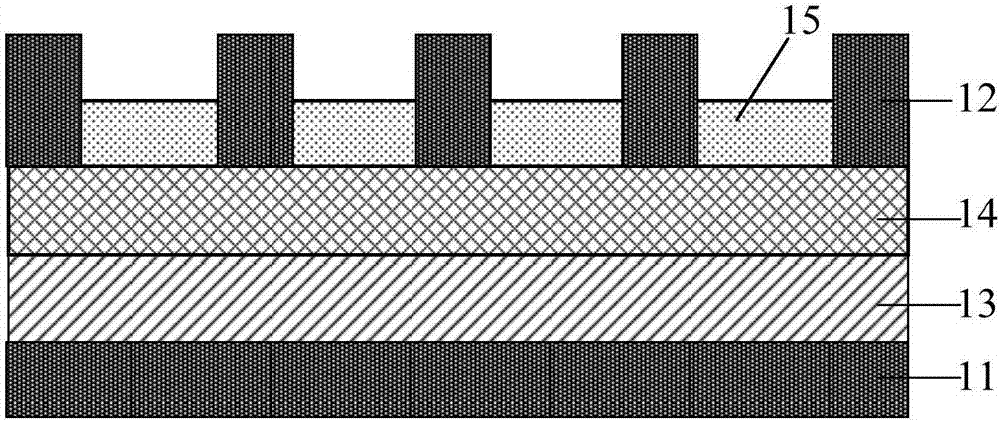
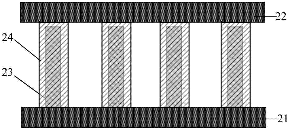
[0035] On the one hand, embodiments of the present invention provide a solar cell, such as figure 2 shown, including:

[0036] The first substrate 1 and the second substrate 2 arranged oppositely;

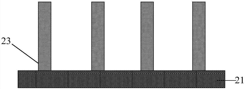
[0037] A plurality of PN junctions arranged between the first substrate 21 and the second substrate 22, each PN junction connects the first substrate 21 and the second substrate 22, and respectively includes: an inner core 23 as a P electrode, and an inner core 23 as an N electrode And cover the cladding layer 24 of the inner core 23 .

[0038] The PN junction of the solar cell of this embodiment is that the N electrode surrounds the P electrode. This ...


PUM


Abstract

The invention provides a solar cell, a solar cell manufacturing method, and electric equipment. The solar cell includes a first substrate and a second substrate disposed opposite to each other; and a plurality of PN junctions disposed between the first substrate and the second substrate, each PN junction being connected with the first substrate and the second substrate and including an inner core as a P electrode and a cladding layer as an N electrode and covering the inner core. According to the invention, the PN junctions of the solar cell are formed by encircling the P electrodes with the N electrodes and such structural design can increase the contact area between the N electrodes and the P electrodes, so that electrons can be quickly separated from empty holes and transmitted and the utilization of solar cells is effectively improved; and in addition, the PN junctions of the embodiment can reduce the reflection area of the light compared to the PN junctions of a laminated structure in the prior art, thus, no anti-reflection layer is required, and manufacturing procedures and the production cost are reduced.

Description

technical field [0001] The invention relates to the technical field of batteries, in particular to a solar battery, a manufacturing method of the solar battery and electrical equipment. Background technique [0002] Such as figure 1 As shown, the structure of a traditional silicon solar cell mainly includes: a front electrode 11, a back electrode 12, a P-type semiconductor (that is, a P-type semiconductor electrode, referred to as a P electrode) 13 and an N-type semiconductor 14 (that is, an N-type semiconductor electrode, referred to as the N electrode). At the same time, in order to reduce the light reflection of the semiconductor silicon crystal, an anti-reflection layer 15 is added on the surface of the semiconductor in the prior art to ensure that the solar cell can fully absorb light energy. [0003] However from figure 1 It can be seen from the figure that the existing solar cell adopts the lamination structure of the P-type semiconductor 13 and the N-type semicond...

Claims


Application Information

Patent Timeline
Patent Type & Authority Applications(China)
IPC IPC(8): H01L31/0352H01L31/0725H01L31/18
CPCH01L31/03529H01L31/0725H01L31/18B82Y30/00H01L21/02491H01L21/02554H01L21/02603H01L21/0262H01L29/0676H01L29/068H01L31/022425H01L31/022483H01L31/035227H01L31/035281H01L31/072Y02E10/50H01L31/0336H01L31/1864Y02P70/50
Inventor 王利忠
Owner BOE TECH GRP CO LTD
Why Eureka
Try Eureka