

PCB (Printed Circuit Board) layer layout method and system
A technology of PCB board and layout method, applied in the field of PCB board layer layout method system, can solve the problems of prolonging the design cycle, increasing labor costs, affecting the overall design progress of the project, etc.
- Summary
- Abstract
- Description
- Claims
- Application Information
AI Technical Summary
Problems solved by technology
Method used
Image

Examples
Embodiment Construction
[0040] In order to make the object, technical solution and advantages of the present invention clearer, the present invention will be further described in detail below in conjunction with the accompanying drawings and embodiments. It should be understood that the specific embodiments described here are only used to explain the present invention, not to limit the present invention.
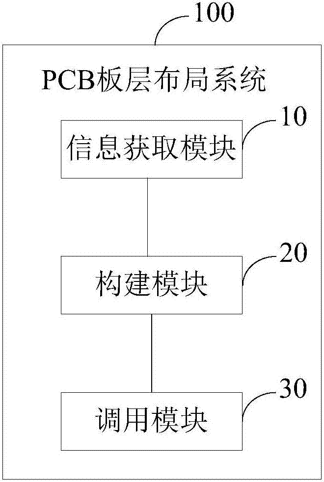
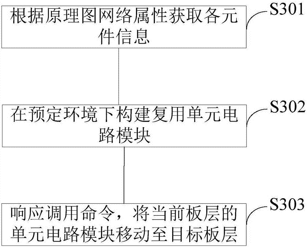
[0041] The technical method involves inversion of element layout and wiring levels due to designer's negligence when using Cadence allegro design software for pcb layout and wiring. At this time, if the design is modified according to the conventional method, a lot of time and energy will be wasted. For this reason, a skillful method for quickly switching the layout and wiring of the top and bottom layers (or local unit circuit modules) is proposed.
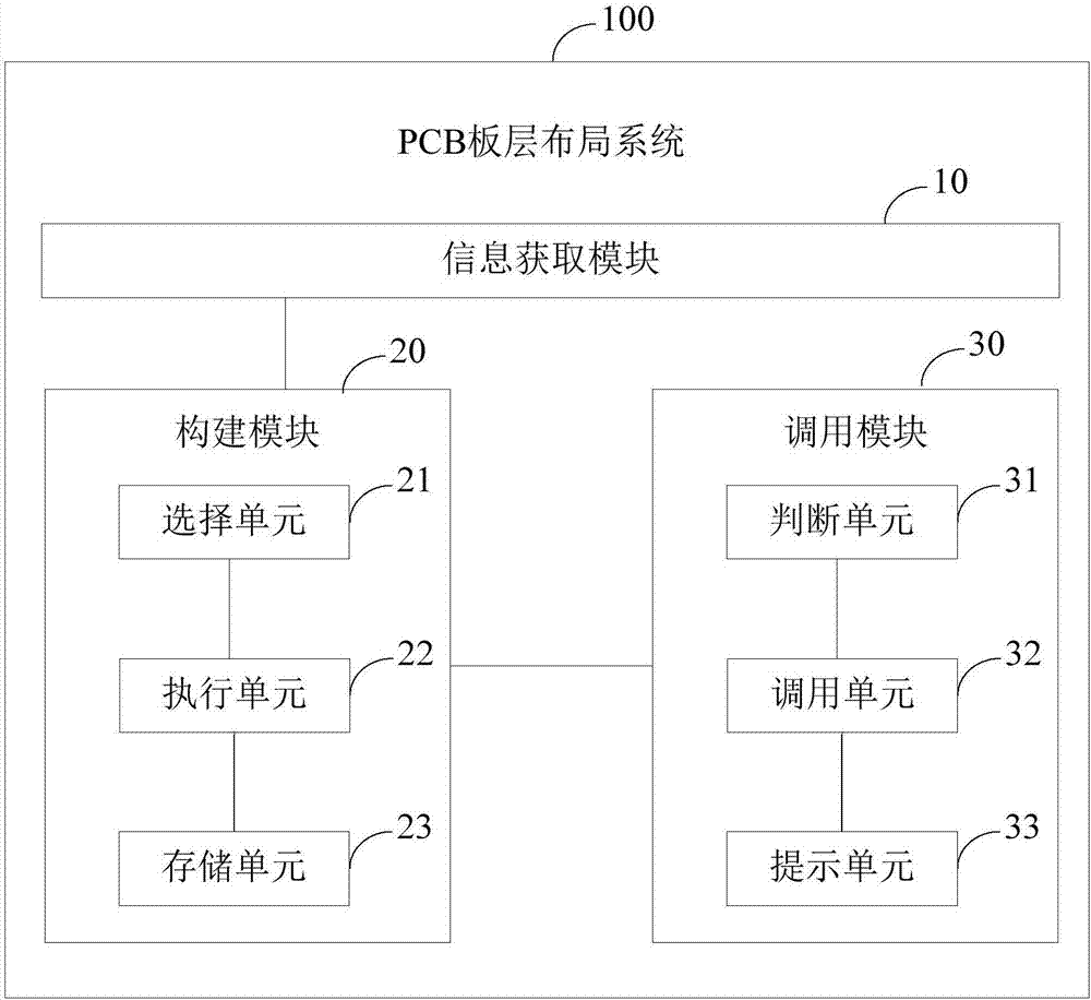
[0042] see figure 1 , the present invention provides a PCB board layer layout system, which includes an information acquisition module 10, a buildin...
PUM
 Abstract
Description
Claims
Application Information