Silicon-based germanium photodetector

A photodetector, silicon-based technology, applied in the field of photodetectors, can solve problems such as improving the comprehensive performance index of the device and increasing the bandwidth, and achieve the effects of improving the comprehensive performance index, increasing the bandwidth, and reducing the dark current.

Inactive Publication Date: 2017-01-11
ZTE CORP
View PDF10 Cites 32 Cited by
  • Summary
  • Abstract
  • Description
  • Claims
  • Application Information

AI Technical Summary

Problems solved by technology

In short, among the waveguide-integrated silicon-based germanium photodetectors known so far, there is no device that can increase the bandwidth under the premise of suppressing the dark current, and it is difficult to improve the comprehensive performance index of the device as a whole.

Method used


Image

  • Silicon-based germanium photodetector
  • Silicon-based germanium photodetector
  • Silicon-based germanium photodetector

Examples


Embodiment Construction

[0022] It should be understood that the specific embodiments described here are only used to explain the present invention, not to limit the present invention.

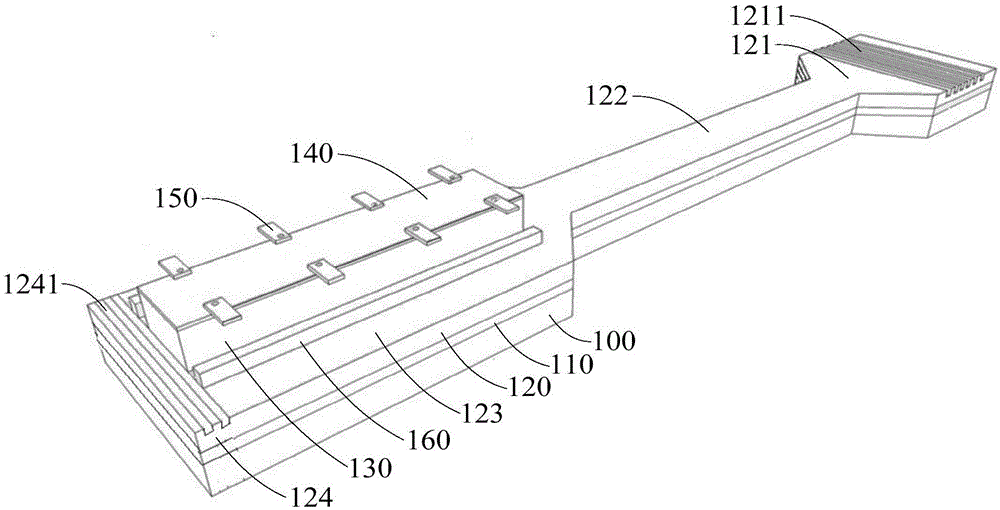
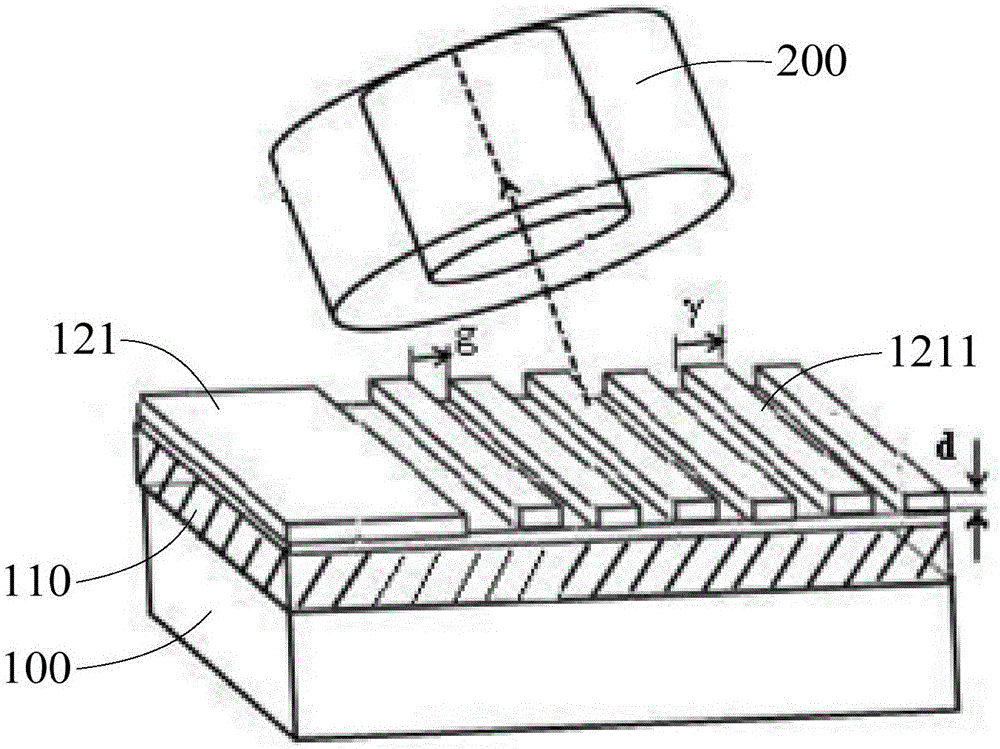
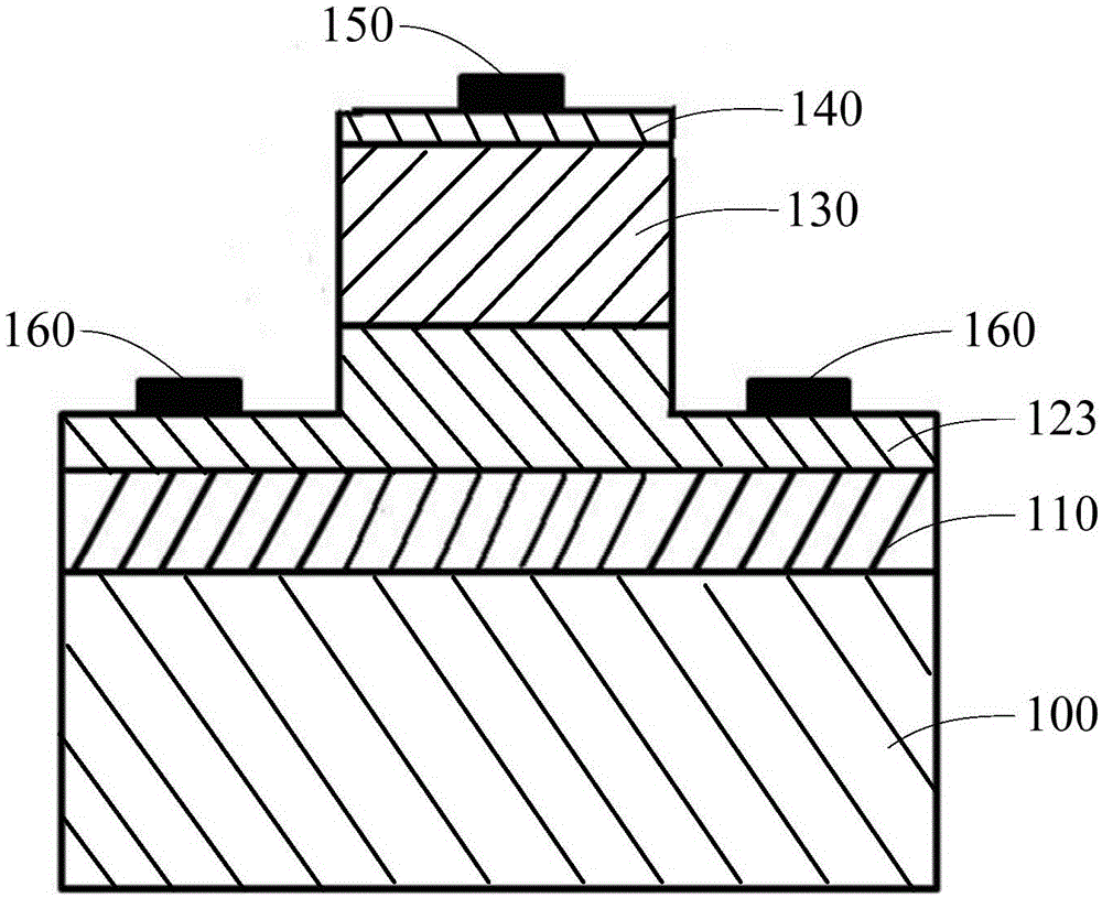
[0023] The invention provides a silicon-based germanium photodetector, see Figure 1 to Figure 3 , in one embodiment, the germanium-on-silicon photodetector includes an optical waveguide layer 120, a silicon oxide layer 110 and a silicon substrate 100 sequentially stacked from top to bottom, wherein the silicon substrate 100 is an insulator made of silicon material , the silicon oxide layer 110 can be grown on the silicon substrate 100. For example, the silicon oxide layer 110 is made of silicon dioxide, and of course it can also be any other suitable compound semiconductor material. Similarly, on the silicon oxide layer 110 The optical waveguide layer 120 is grown, and the optical waveguide layer 120 is a silicon structure formed on the silicon oxide layer 110, which is used to receive optical signals and guide the p...


PUM


Abstract

The present invention discloses a silicon-based germanium photodetector. The silicon-based germanium photodetector comprises an optical waveguide layer, a silicon oxide layer and a silicon substrate which are sequentially stacked from top to bottom; the optical waveguide layer includes an optical coupling region, a planar optical waveguide region and an optical output region which are distributed sequentially along the propagation direction of optical signals; a coupling grating for receiving the optical signals and guiding the optical signals to the planar optical waveguide region is formed in the coupling region; and the silicon-based germanium photodetector further comprises a germanium layer stacked on the optical output region, a silicon covering layer stacked on the germanium layer, a first electrode formed on the silicon covering layer, and a second electrode formed on the optical output region, wherein the germanium layer receives the optical signals from the optical output region and converts the optical signals into electrical signals. According to the silicon-based germanium photodetector of the invention, the silicon covering layer is adopted, so that bandwidth is greatly improved, the dark current of the device is greatly reduced, and therefore, the comprehensive performance index of the device can be improved, and the requirements of high-speed optical communication and optical interconnection systems can be better satisfied.

Description

technical field [0001] The invention relates to the technical field of photodetectors, in particular to a silicon-based germanium photodetector. Background technique [0002] In semiconductor photodetectors, when the photodetector is exposed to a light source, the photodetector absorbs light energy through the detection material and converts it into an electronic signal to output current, which can be used for optical communication and light detection. [0003] As one of the important representatives of silicon-based optoelectronic integration technology, silicon-based germanium photodetectors have been continuously optimized in structure and further improved in performance after decades of development. Depending on the angle of incidence of their light, photodetectors can be classified into two types, normal incidence (free space) and edge incidence (waveguide integration). In the waveguide integrated photodetector, since the propagation and absorption of light are along t...

Claims


Application Information

Patent Timeline
Patent Type & Authority Applications(China)
IPC IPC(8): H01L31/101
CPCH01L31/101
Inventor 周治平涂芝娟华锋王会涛张琦
Owner ZTE CORP
Why Eureka
Try Eureka