Protective film covering method
A technology of protective film and wafer, applied in the direction of electrical components, lasers, electric solid-state devices, etc., can solve the problems of detachment, inability to perform smooth laser processing, etc., and achieve the effect of effective removal and improved cleaning effect.
- Summary
- Abstract
- Description
- Claims
- Application Information
AI Technical Summary
Problems solved by technology
Method used
Image


Examples
Embodiment Construction
[0030] Hereinafter, preferred embodiments of the protective film coating method of the present invention will be described in detail with reference to the drawings.
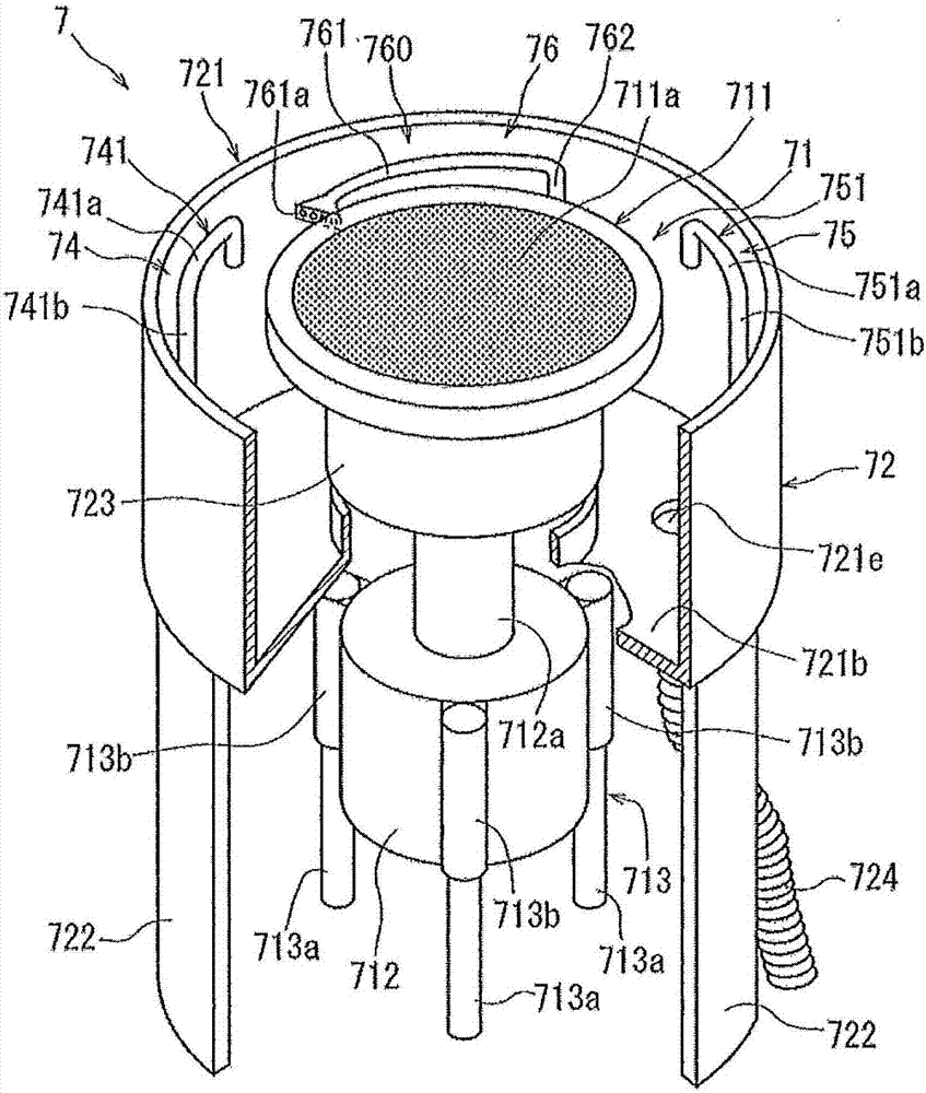
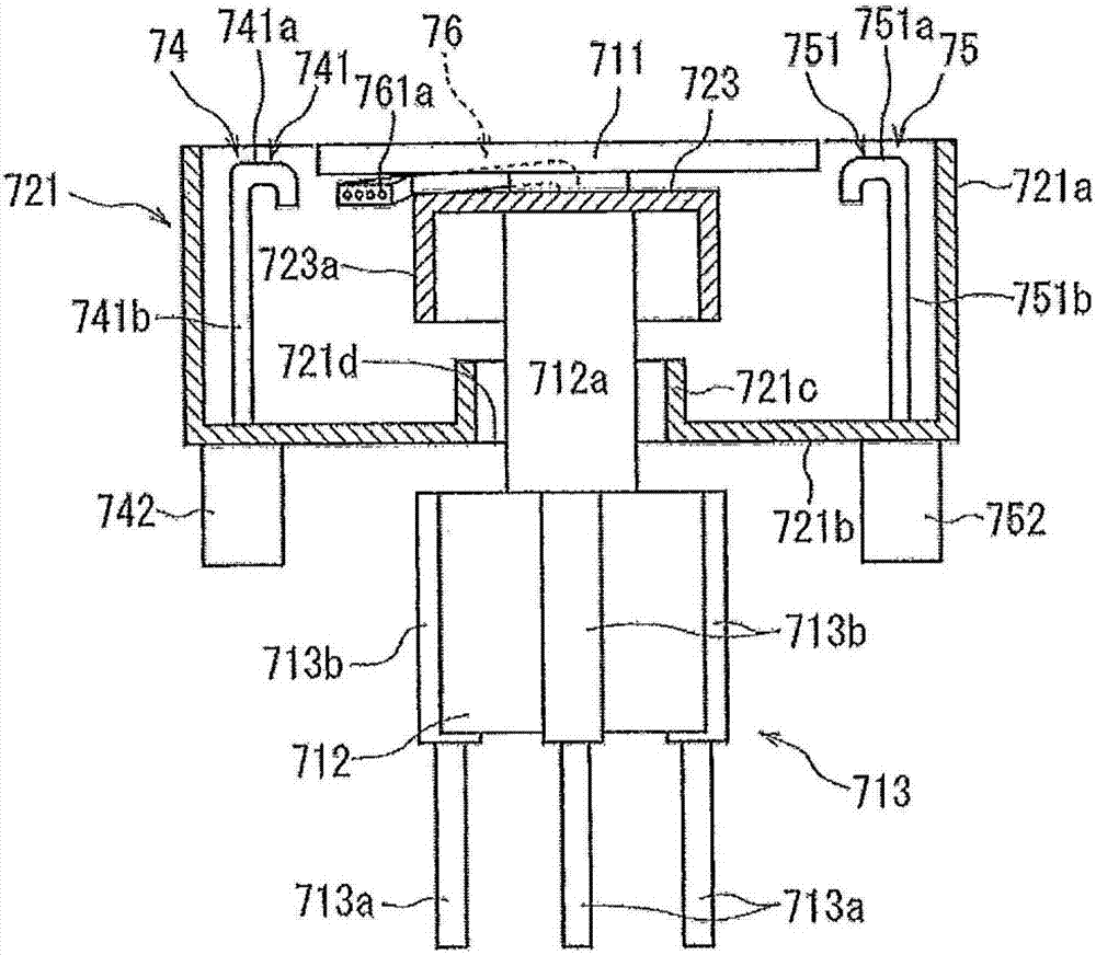
[0031] exist figure 1 A perspective view of a laser processing machine equipped with a protective film covering device for carrying out the protective film covering method of the present invention is shown in .
[0032] figure 1 The laser processing machine 1 shown has an approximately cuboid device housing 2 . A chuck table 3 as a workpiece holding unit for holding a workpiece is disposed in the device housing 2, and the chuck table 3 can move in the direction indicated by the arrow X as the cutting feed direction. move. The chuck table 3 has a suction chuck support table 31 and a suction chuck 32 mounted on the suction chuck support table 31, and holds, for example, a disk-shaped semiconductor wafer as a workpiece by a suction unit not shown in the figure. It is held on the mounting surface which is the fro...
PUM
 Abstract
Description
Claims
Application Information
 - Generate Ideas
- Intellectual Property
- Life Sciences
- Materials
- Tech Scout
- Unparalleled Data Quality
- Higher Quality Content
- 60% Fewer Hallucinations
Browse by: Latest US Patents, China's latest patents, Technical Efficacy Thesaurus, Application Domain, Technology Topic, Popular Technical Reports.
© 2025 PatSnap. All rights reserved.Legal|Privacy policy|Modern Slavery Act Transparency Statement|Sitemap|About US| Contact US: help@patsnap.com