Aluminum gallium nitride (AlGaN)base solar-blind ultraviolet detector and preparation method thereof
An ultraviolet detector, AlGaN technology, applied in semiconductor devices, final product manufacturing, sustainable manufacturing/processing, etc., can solve the problems of low quality of AlGaN material films, restricting the detection performance of structural detectors, and large dark current. , to achieve the effect of improving quantum efficiency and responsivity, reducing avalanche breakdown voltage threshold, and increasing electric field
- Summary
- Abstract
- Description
- Claims
- Application Information
AI Technical Summary
Problems solved by technology
Method used
Image

Examples
Embodiment 1
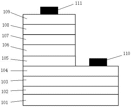
[0031] Example 1, such as figure 1 As shown, the AlGaN-based solar-blind ultraviolet detector involved in this embodiment includes a patterned C-plane oriented sapphire substrate 101, an AlN nucleation layer 102, an Al x1 Ga 1-x1 N buffer layer 103, n-type Al x2 Ga 1-x2 N layer 104, non-doped i-type Zn y1 Mg 1-y1 O absorption layer 105, n-type ZnO / Zn y2 Mg 1-y2 O superlattice separation layer 106, non-doped i-type Zn y3 Mg 1-y3 O multiplication layer 107, p-type Al x3 Ga 1-x3 N layer 108, p-type GaN layer 109, in n-type Al x2 Ga 1-x2 The n-type ohmic electrode 110 drawn out from the N layer 104 and the p-type ohmic electrode 111 drawn out on the p-type GaN layer 109 . The thickness of the AlN nucleation layer 102 is 30 nm, and the specific thickness of the nucleation layer can be adjusted according to actual needs. al x1 Ga 1-x1 The thickness of the N buffer layer 103 is 500 nm, and x1=0.35 therein. n-type Al x2 Ga 1-x2 The thickness of the N layer 104 is 800...
Embodiment 2
[0044] Example 2, such as figure 1 As shown, the AlGaN-based solar-blind ultraviolet detector involved in this embodiment includes a patterned C-plane oriented sapphire substrate 101, an AlN nucleation layer 102, an Al x1 Ga 1-x1 N buffer layer 103, n-type Al x2 Ga 1-x2 N layer 104, non-doped i-type Zn y1 Mg 1-y1 O absorption layer 105, n-type ZnO / Zn y2 Mg 1-y2 O superlattice separation layer 106, non-doped i-type Zn y3 Mg 1-y3 O multiplication layer 107, p-type Al x3 Ga 1-x3 N layer 108, p-type GaN layer 109, in n-type Al x2 Ga 1-x2 The n-type ohmic electrode 110 drawn out from the N layer 104 and the p-type ohmic electrode 111 drawn out on the p-type GaN layer 109 . The thickness of the AlN nucleation layer 102 is 20 nm, and the specific thickness of the nucleation layer can be adjusted according to actual needs. al x1 Ga 1-x1 The thickness of the N buffer layer 103 is 200 nm, and x1=0.4 therein. n-type Al x2 Ga 1-x2 The thickness of the N layer 104 is 500n...
Embodiment 3
[0045] Example 3, such as figure 1 As shown, the AlGaN-based solar-blind ultraviolet detector involved in this embodiment includes a patterned C-plane oriented sapphire substrate 101, an AlN nucleation layer 102, an Al x1 Ga 1-x1 N buffer layer 103, n-type Al x2 Ga 1-x2 N layer 104, non-doped i-type Zn y1 Mg 1-y1 O absorption layer 105, n-type ZnO / Zn y2 Mg 1-y2 O superlattice separation layer 106, non-doped i-type Zn y3 Mg 1-y3 O multiplication layer 107, p-type Al x3 Ga 1-x3 N layer 108, p-type GaN layer 109, in n-type Al x2 Ga 1-x2 The n-type ohmic electrode 110 drawn out from the N layer 104 and the p-type ohmic electrode 111 drawn out on the p-type GaN layer 109 . The thickness of the AlN nucleation layer 102 is 50 nm, and the specific thickness of the nucleation layer can be adjusted according to actual needs. al x1 Ga 1-x1 The thickness of the N buffer layer 103 is 400 nm, and x1=0.5 therein. n-type Al x2 Ga 1-x2The thickness of the N layer 104 is 1000n...
PUM
| Property | Measurement | Unit |
|---|---|---|
| Thickness | aaaaa | aaaaa |
| Thickness | aaaaa | aaaaa |
| Thickness | aaaaa | aaaaa |
Abstract
Description
Claims
Application Information
 - R&D
- Intellectual Property
- Life Sciences
- Materials
- Tech Scout
- Unparalleled Data Quality
- Higher Quality Content
- 60% Fewer Hallucinations
Browse by: Latest US Patents, China's latest patents, Technical Efficacy Thesaurus, Application Domain, Technology Topic, Popular Technical Reports.
© 2025 PatSnap. All rights reserved.Legal|Privacy policy|Modern Slavery Act Transparency Statement|Sitemap|About US| Contact US: help@patsnap.com