Aluminum gallium nitrogen-based solar blind ultraviolet detector and production method thereof

An ultraviolet detector, aluminum gallium nitride technology, applied in semiconductor devices, electrical components, circuits, etc., can solve the problems of restricting the detection performance of structural detectors, large dark current, and low film quality, and improve quantum efficiency and responsivity. , the effect of increasing the sensitivity and improving the quality of the device

Inactive Publication Date: 2015-02-18
SOUTHEAST UNIV
View PDF11 Cites 29 Cited by
  • Summary
  • Abstract
  • Description
  • Claims
  • Application Information

AI Technical Summary

Problems solved by technology

[0005] However, due to the low quality of the AlGaN material film prepared by the prior art, there are a large number of defects in the interface between the AlGaN material and the metal deposited on the surface when it forms a Schottky junction, which makes the active region thinner and the tunneling mechanism is obvious, resulting in dark The current is very large, which severely restricts the improvement of the detection performance of this type of structure detector [Reference: AlGaNSchottky Diodes for Detector Applications in the UV Wavelength Range. IEEE Trans. Electron Devices 56, 2833(2009).]

Method used


Image

  • Aluminum gallium nitrogen-based solar blind ultraviolet detector and production method thereof
  • Aluminum gallium nitrogen-based solar blind ultraviolet detector and production method thereof

Examples


Embodiment Construction

[0032] The present invention will be further described below in conjunction with the accompanying drawings.

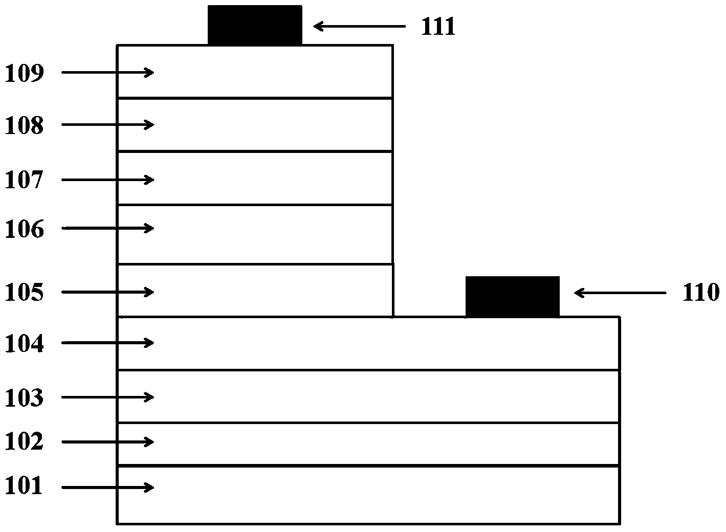
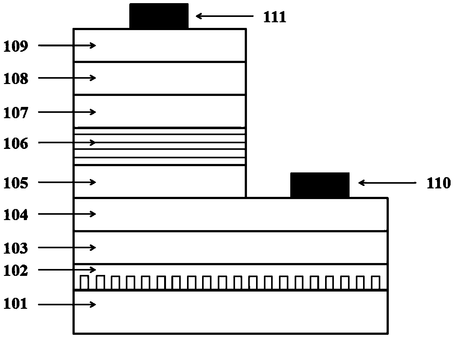
[0033] Such as figure 2 Shown is an AlGaN-based solar-blind ultraviolet detector, including a sapphire substrate 101, an AlN nucleation layer 102, an Al x1 Ga 1-x1 N buffer layer 103, n-type Al x2 Ga 1-x2 N layer 104, undoped i-type Al x3 Ga 1-x3 N absorption layer 105, n-type Al x4 In y1 Ga 1-x4-y1 N / Al x5 In y2 Ga 1-x5-y2 N superlattice separation layer 106, non-doped i-type Al x6 Ga 1-x6 N multiplication layer 107, p-type Al x7 Ga 1-x7 N layer 108 and p-type GaN layer 109, in n-type Al x2 Ga 1-x2 An n-type ohmic electrode (110) is drawn out on the N layer 104, and a p-type ohmic electrode (111) is drawn out on the p-type GaN layer 109.

[0034] The sapphire substrate 101 is a double-sided polished C-plane crystal and has sub-micron patterned C-plane crystals; the specifications and dimensions of the sapphire substrate 101 are: bottom width 100-1000...


PUM


Abstract

The invention discloses an aluminum gallium nitrogen-based solar blind ultraviolet detector and a production method thereof. The aluminum gallium nitrogen-based solar blind ultraviolet detector comprises a sapphire substrate, an A1N nucleating layer, an A1<x1>Ga<1-x1>N buffer layer, an n-type A1<x2>Ga<1-x2>N layer, an undoped i-type A1<x3>Ga<1-x3>N absorbing layer, an n-type A1<X4>In<y1>Ga<1-x4-y1>N / A1<x5>In<y2>Ga<1-x5-y2>N superlattice separating layer, an undoped i-type A1<x6>Ga<1-x6>N multiplication layer, a p-type A1<x7>Ga<1-x7>N layer and a p-type GaN layer which are sequentially arranged from the bottom up. An n-type ohmic electrode leads from the n type A1<x2>Ga<1-x2>N layer, and a p type ohmic electrode leads from the p type GaN layer. According to the arrangement, the absorbing layer and the multiplication layer are separated by the multi-cycle n type A1<X4>In<y1>Ga<1-x4-y1>N / A1<x5>In<y2>Ga<1-x5-y2>N superlattice separating layer, the electric field of the multiplication layer is increased, thus allowing uniform avalanche multiplication to occur under the high electric field, and avalanche multiplication factors of the solar blind ultraviolet detector are increased.

Description

technical field [0001] The invention relates to the field of semiconductor optoelectronic devices, in particular to an aluminum gallium nitrogen-based solar-blind ultraviolet detector and a preparation method thereof. Background technique [0002] Gallium nitride-based semiconductor materials mainly include binary compounds GaN, InN, AlN of group III and group V elements, ternary compounds InGaN, AlGaN, AlInN and quaternary compounds AlInGaN, which have a large band gap, high thermal conductivity, and High temperature, radiation resistance, acid and alkali resistance, high strength and high hardness and other characteristics, in high-brightness blue, green, purple, ultraviolet and white light-emitting diodes (LEDs), blue and purple lasers and radiation resistance, high temperature resistance, high-power microwave devices And other fields have a wide range of application potential and good market prospects. Ternary compound Al x Ga 1-x The energy band gap of N can be adjus...

Claims


Application Information

Patent Timeline
Patent Type & Authority Applications(China)
IPC IPC(8): H01L31/107H01L31/0352H01L31/036H01L31/108
CPCH01L31/035209H01L31/035236H01L31/036H01L31/1075H01L31/108
Inventor 张雄王书昶崔一平
Owner SOUTHEAST UNIV
Why Eureka
Try Eureka