Semiconductor film laminating machine

A semiconductor and laminating machine technology, applied in semiconductor devices, semiconductor/solid-state device manufacturing, semiconductor/solid-state device testing/measurement, etc., can solve problems such as error-prone, increased labor costs, loss, etc., to improve efficiency and reduce labor Cost, the effect of realizing the film sticking operation

Pending Publication Date: 2017-07-21
DONGGUAN ANDA AUTOMATIC EQUIP
View PDF4 Cites 6 Cited by
  • Summary
  • Abstract
  • Description
  • Claims
  • Application Information

AI Technical Summary

Problems solved by technology

[0003] The existing method of attaching films to semiconductors is through manual film attachment, and the existing processing methods mainly have the following problems: However, due to the increasing demand for semiconductors, the number of workers who need to transport and transport semiconductors needs to gradually increase ,

Method used


Image

  • Semiconductor film laminating machine
  • Semiconductor film laminating machine
  • Semiconductor film laminating machine

Examples


Embodiment Construction

[0030] The present invention is further described in conjunction with the following examples.

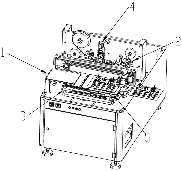
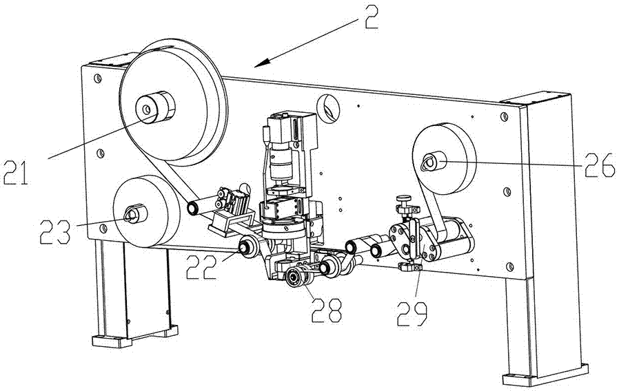
[0031] A laminating machine for semiconductor film sticking described in this embodiment, such as figure 1 As shown, it includes a retrieving device 1 for loading and unloading operations on the semiconductor carrier, a film attaching device 2 for attaching films to multiple semiconductors on the semiconductor carrier, and reciprocating between the retrieving device 1 and the film attaching device 2 for moving Material transfer device 3 for semiconductor loading. Such as figure 1 As shown, when it is necessary to carry out film-attaching operations on multiple semiconductors on the semiconductor carrier, the semiconductor carrier can be automatically moved by the pick-up device 1 to the semiconductor carrier and the material transfer device 3 to move back and forth on the semiconductor carrier. Complete the loading and unloading operation. In addition, a detection device 4 for de...


PUM


Abstract

The invention relates to the technical field of film pasting devices, and specifically relates to a semiconductor film laminating machine. The machine comprises a fetching device which is used for carrying out the feeding and laying-off operation of a semiconductor carrying disc, a film pasting device for pasting films on a plurality of semiconductors on the semiconductor carrying disc, and a material moving device which moves between the fetching device and the film pasting device and is used for moving semiconductors. A detection device for detecting the position of the semiconductor carrying disc and a position adjustment device for adjusting the positions of the semiconductors carrying disc are disposed between the material moving device and the film pasting device. The position adjustment device is movably connected with the material moving device. The machine achieves the automatic conveying of semiconductors at multiple angles through the fetching device and the material moving device, reduces the cost, and guarantees the stable conveying of the semiconductors. The positions of the semiconductors are adjusted through the detection device and the position adjustment device, and the machine can enable the semiconductors to face the film pasting device, and guarantees the film pasting quality. The machine achieves the automatic pasting of films for the semiconductors through the film pasting device, and improves the film pasting efficiency.

Description

technical field [0001] The invention relates to the technical field of film sticking devices, in particular to a laminating machine for semiconductor film sticking. Background technique [0002] A semiconductor refers to a material whose conductivity is between that of a conductor and an insulator at room temperature. In today's intelligent era, the development of communications, computers and the Internet of Things is closely related to the use of semiconductors, which gradually affect human technological progress and economic development. The demand for semiconductors in the market is growing explosively. Due to the limitations of the semiconductor structure, it is easy to damage the semiconductor due to scratches or other means and cannot be used normally. Therefore, in daily protection, the semiconductor needs to be treated with a film. [0003] The existing method of attaching films to semiconductors is through manual film attachment, and the existing processing metho...

Claims


Application Information

Patent Timeline
IPC IPC(8): H01L21/673H01L21/677H01L21/68H01L21/66B65B33/02
CPCH01L21/673H01L21/67763H01L21/68H01L22/20B65B33/02H01L2221/683H01L2221/67
Inventor 刘飞
Owner DONGGUAN ANDA AUTOMATIC EQUIP
Why Eureka
Try Eureka