Semiconductor structure, forming method thereof and test method

A test method and semiconductor technology, applied in semiconductor/solid-state device testing/measurement, semiconductor device, semiconductor/solid-state device manufacturing, etc., can solve problems such as poor yield rate of MOS transistors, improve yield rate, ensure purity, and avoid whitening The effect of point defects

A test method and semiconductor technology, applied in semiconductor/solid-state device testing/measurement, semiconductor device, semiconductor/solid-state device manufacturing, etc., can solve problems such as poor yield rate of MOS transistors, improve yield rate, ensure purity, and avoid whitening The effect of point defects

CN106997900AInactive Publication Date: 2017-08-01SEMICON MFG INT (SHANGHAI) CORP +1

Image

  • Semiconductor structure, forming method thereof and test method
  • Semiconductor structure, forming method thereof and test method
  • Semiconductor structure, forming method thereof and test method

Examples


Embodiment Construction

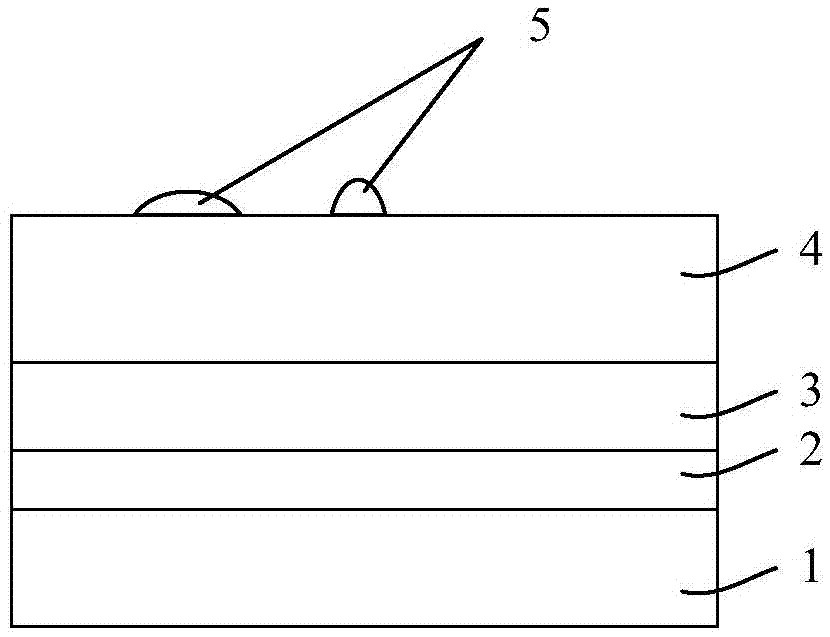
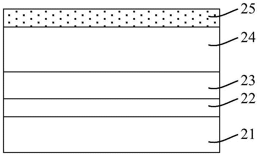
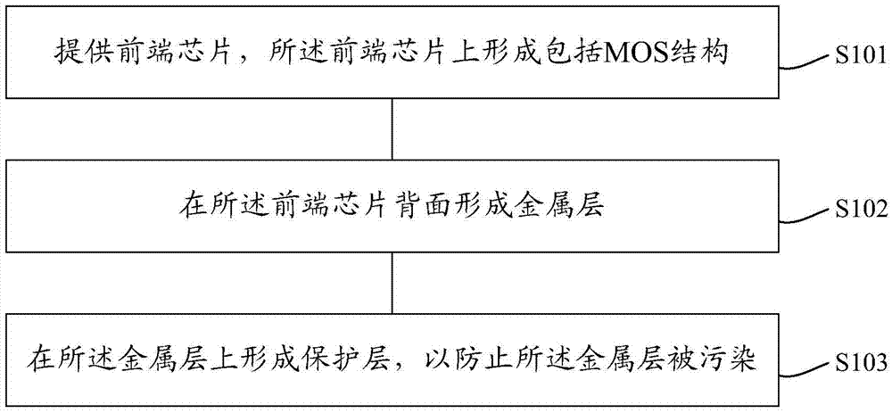
[0035] The semiconductor structure of the present invention, its forming method and testing method will be described in more detail below in conjunction with schematic diagrams, wherein a preferred embodiment of the present invention is represented, and it should be understood that those skilled in the art can modify the present invention described here, and still realize Advantageous effects of the present invention. Therefore, the following description should be understood as the broad knowledge of those skilled in the art, but not as a limitation of the present invention.

[0036] In the following paragraphs the invention is described more specifically by way of example with reference to the accompanying drawings. Advantages and features of the present invention will be apparent from the following description and claims. It should be noted that all the drawings are in a very simplified form and use imprecise scales, and are only used to facilitate and clearly assist the pu...


PUM


Abstract

The invention discloses a semiconductor structure, a forming method thereof and a test method. The semiconductor structure comprises a front-end chip, a metal layer located on the back surface of the front-end chip and a protection layer located on the metal layer, wherein the protection layer can protect the metal layer from being polluted. Thereby, the protection layer is used to protect the metal layer on the semiconductor structure from being oxidized by air, moisture and other substances, and generation of white spot defects is avoided. In the case of test, the protection layer can be removed, the test can be carried out normally, and the product yield can be improved.

Description

technical field [0001] The invention relates to the technical field of semiconductor manufacturing, in particular to a semiconductor structure, its forming method and testing method. Background technique [0002] With the continuous development of semiconductor technology, integrated circuits have grown from a few interconnected devices fabricated on a single chip to millions of devices. Current integrated circuits offer increasing performance and complexity. Metal-oxide-semiconductor (MOS) transistors are the most basic devices in semiconductor manufacturing, and are widely used in various integrated circuits. Therefore, the industry has never stopped improving and optimizing the performance of MOS transistors. [0003] At present, in order to improve the electrical performance of MOS transistors, Backside Grinding Backside Metal (BGBM) technology has been applied to the manufacturing process of MOS transistors and has become a key link. This technology is to form a metal...

Claims


Application Information

Patent Timeline
01 Aug 2017
Publication
CN106997900A
IPC
H01L29/78; H01L21/336; H01L21/66
CPC
H01L29/66477; H01L29/78; H01L22/14
Inventors
陈彧