

Test tray for test handler and interface board for tester
A technology for testing sorting machines and test trays, which is applied in the direction of single semiconductor device testing, electrical measuring instrument components, sorting, etc., and can solve the problem of removing calibration pins from calibration holes, and the electrical connection between semiconductor components and test sockets. Achievement, restriction and other issues, to achieve the effect of minimizing assembly tolerances
- Summary
- Abstract
- Description
- Claims
- Application Information
AI Technical Summary
Problems solved by technology
Method used
Image

Examples
Embodiment 1
[0061] 1. Test tray for testing sorting machine
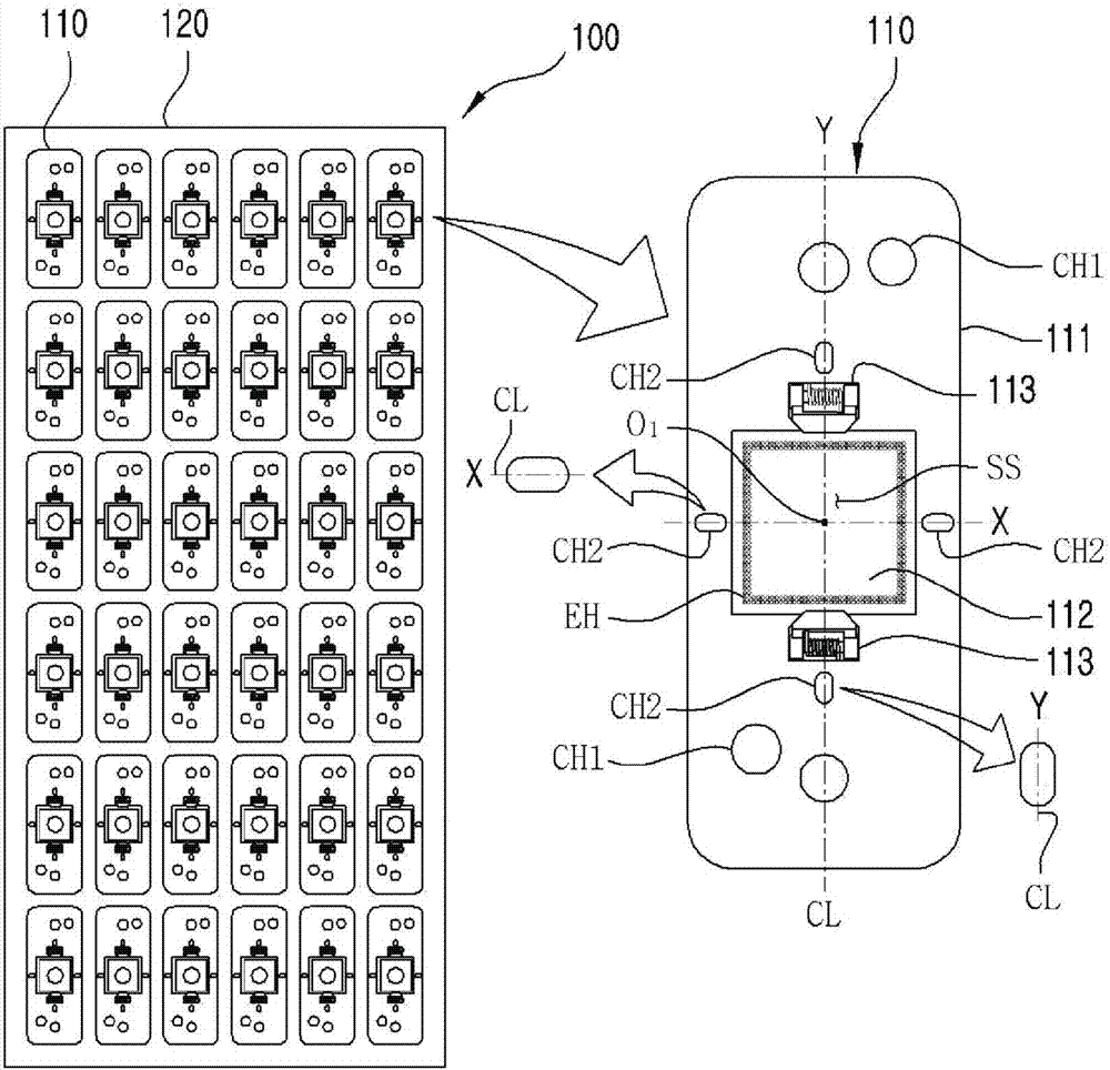
[0062] figure 1 is a plan view of a test tray 100 (hereinafter referred to as "test tray") for testing a sorter according to a first embodiment of the present invention.
[0063] The test tray 100 according to the first embodiment includes a plurality of inserts 110 and a mounting frame 120 .
[0064] Each of the inserts 110 includes a body 111 , a support member 112 and a retainer 113 .
[0065] The body 111 has a placement space SS on which a semiconductor element may be placed. In addition, the body 111 has two first calibration holes CH1 and four second calibration holes CH2.
[0066] The first correction hole CH1 is formed to have an inner diameter in consideration of manufacturing tolerances, which has been described in [Prior Art]. The first calibration hole CH1 is used to firstly correct the position of the insert 110 .
[0067] The second correction hole CH2 is formed to secondly and more accurately correct the ...
Embodiment 2
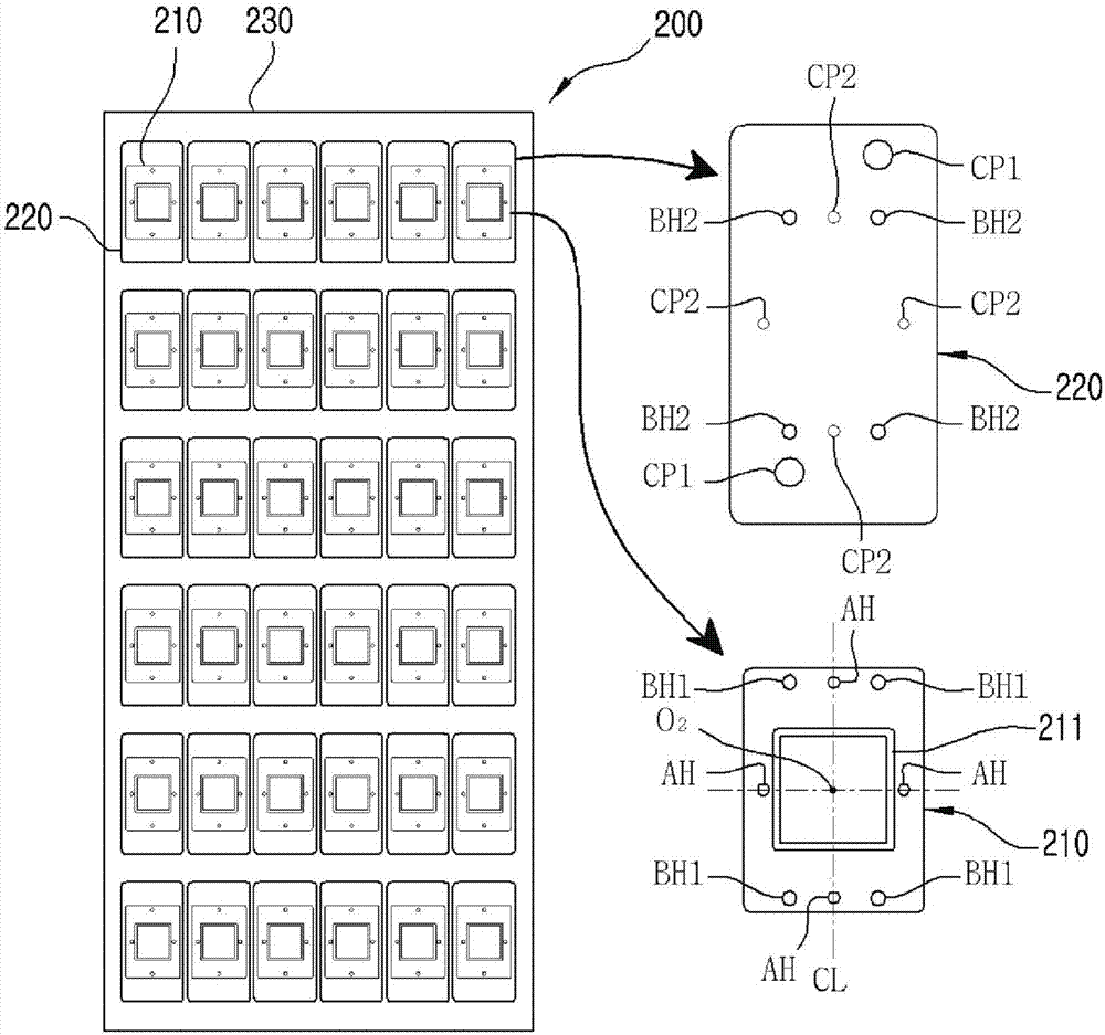
[0099] Figure 8 is a plan view of a test tray 700 for a test sorter (hereinafter referred to as "test tray") according to a second embodiment of the present invention.
[0100] In this embodiment, the test tray 700 includes a plurality of inserts 710 and a mounting frame 720 .
[0101] The insert 710 includes a body 711 , a support member 712 and a holder 713 . Here, descriptions of the support member 712 and the holder 713 will be omitted since they are the same components as those of the first embodiment.
[0102] The body 711 has a placement space SS on which a semiconductor element is placed. In addition, the body 711 has a correction hole CH and a cutout hole IH.
[0103] The position of the insert 710 is corrected because a correction pin of the interface board (the same as the first correction pin in the first embodiment) is inserted into the correction hole CH. hereby, if Figure 9 As shown in , the wall surface W of the correction hole CH has a cutout portion IP...
PUM
 Abstract
Description
Claims
Application Information