Active matrix substrate and display panel
An active matrix and substrate technology, which is applied in the field of active matrix substrates and display panels, can solve the problems of display quality degradation and display unevenness.
- Summary
- Abstract
- Description
- Claims
- Application Information
AI Technical Summary
Problems solved by technology
Method used
Image


Examples
Embodiment approach 1
[0040] (Structure of liquid crystal display device)
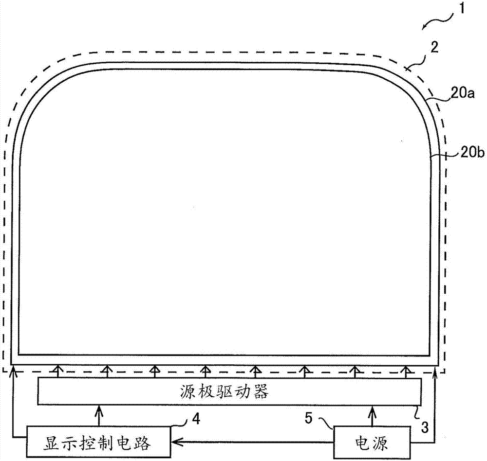
[0041] figure 1 It is a top view showing the schematic configuration of the liquid crystal display device of this embodiment. The liquid crystal display device 1 has a display panel 2 , a source driver 3 , a display control circuit 4 , and a power supply 5 . The display panel 2 has an active matrix substrate 20a, a counter substrate 20b, and a liquid crystal layer (not shown) sandwiched between these substrates. At figure 1 Although the illustration is omitted, polarizers are provided on the lower surface side of the active matrix substrate 20a and the upper surface side of the counter substrate 20b. A black matrix, color filters of three colors of red (R), green (G), and blue (B), and common electrodes (both not shown) are formed on the counter substrate 20b.
[0042] Such as figure 1 As shown, the display panel 2 is formed in an arc shape at the left and right upper end portions in the drawing. That is, the appearan...
Embodiment approach 2
[0102] Figure 13 It is a figure which shows an example of the equivalent circuit of the gate driver 11 in Embodiment 2. Figure 13 The gate driver shown is a gate driver that operates with a four-phase clock (CK). for with Figure 4 The description of the parts that are the same as the equivalent circuits shown is omitted. At Figure 13 In the example shown, the drain and gate of TFT-M1 connected to netA are connected to the gate line GL(n-1) of the preceding stage. In addition, the gate line GL(n+3) after three stages is connected to the gate of TFT-M3. Moreover, the control wiring of the clock signal CKD is connected to the drain and gate of TFT-M8, respectively, and the control wiring of the clock signal CKC is connected to the gate of TFT-M9. In addition, the gate line GL(n−2) two stages before is connected to the gate of TFT-M11.
[0103] Figure 14 is displayed will Figure 13 This is a diagram showing an example of the circuit configuration in the case where th...
Embodiment approach 3
[0112] Figure 18 It is a diagram showing an example of an equivalent circuit of the gate driver 11 in the third embodiment. Figure 18 The gate driver shown is a gate driver operating on an eight-phase clock (CK). for with Figure 4 The description of the parts that are the same as the equivalent circuits shown is omitted. At Figure 18 In the example shown, the drain and gate of TFT-M1 connected to netA are connected to the gate line GL(n−4) four stages before. In addition, the gate line GL(n+4) after 4 stages is connected to the gate of TFT-M3. To the gate of TFT-M11, the gate line GL(n-2) of 4 stages before is connected.
[0113] Figure 18The gate driver 11(n+1) next to the shown gate driver 11(n) is connected to the control lines of the clock signals CKC, CKD instead of the control lines of the clock signals CKA, CKB. The clock signals CKC, CKD may be signals whose phases are shifted by one-eighth wavelength with respect to the clock signals CKA, CKB. Similarly, ...
PUM
 Abstract
Description
Claims
Application Information
 - R&D
- Intellectual Property
- Life Sciences
- Materials
- Tech Scout
- Unparalleled Data Quality
- Higher Quality Content
- 60% Fewer Hallucinations
Browse by: Latest US Patents, China's latest patents, Technical Efficacy Thesaurus, Application Domain, Technology Topic, Popular Technical Reports.
© 2025 PatSnap. All rights reserved.Legal|Privacy policy|Modern Slavery Act Transparency Statement|Sitemap|About US| Contact US: help@patsnap.com