PCB clamping and conveying mechanism and working method thereof

A PCB circuit board, clamping transmission technology, applied in the direction of conveyor objects, transportation and packaging, etc., can solve the problems of processing, PCB circuit board pollution, disadvantages, etc.

Active Publication Date: 2017-08-04
江苏智子自动化科技有限公司
View PDF14 Cites 12 Cited by
  • Summary
  • Abstract
  • Description
  • Claims
  • Application Information

AI Technical Summary

Problems solved by technology

At present, in the PCB circuit board manufacturing process, according to the process of each step, the PCB circuit board needs to be transported from one device to another. Usually, the PCB circuit boards to be processed need to be manually transported to the corresponding workbench one by one, which wastes manpower and The efficiency is low, and at the same time, beca

Method used


Image

  • PCB clamping and conveying mechanism and working method thereof
  • PCB clamping and conveying mechanism and working method thereof
  • PCB clamping and conveying mechanism and working method thereof

Examples


Embodiment 1

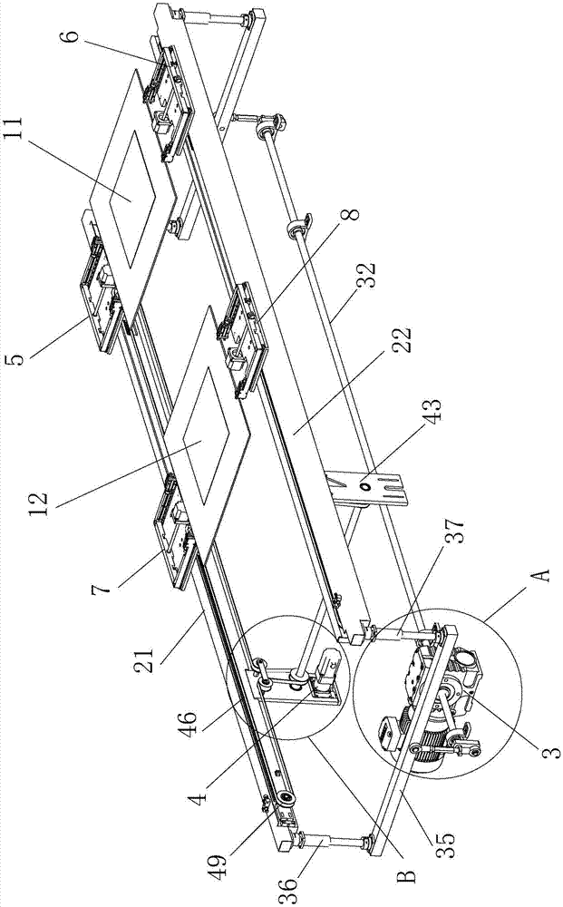
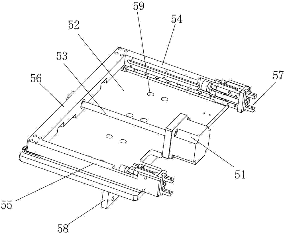
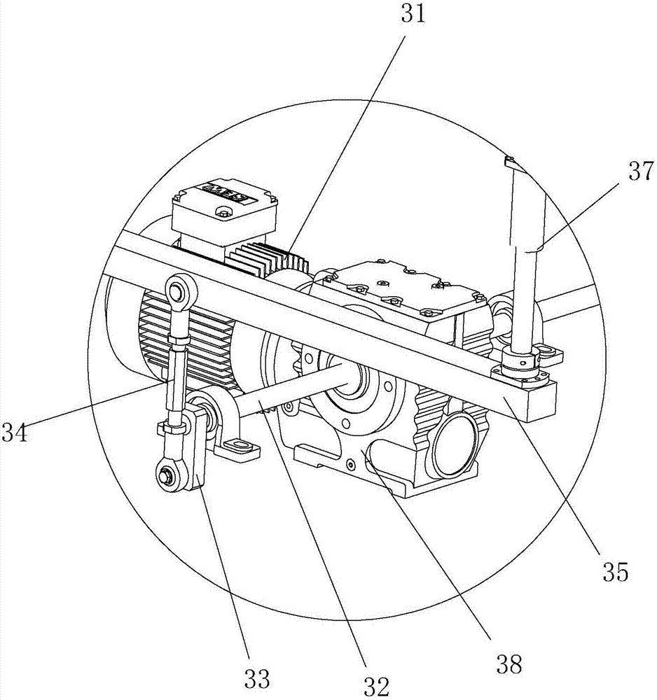
[0024] Example 1 as figure 1 As shown, the PCB circuit board clamping transmission mechanism of this embodiment includes: a left clamping arm support beam 21 and a right clamping arm support beam 22 arranged in parallel, for clamping the first left clamping arm 5 and the first clamping arm 5 of the PCB circuit board. One right clamp arm 6, the second left clamp arm 7, the second right clamp arm 8, the upper end faces of the left clamp arm support beam 21 and the right clamp arm support beam 22 are provided with guide chute respectively, the first left clamp arm 5, the second clamp arm One right jig arm 6, the second left jig arm 7, the second right jig arm 8 are identical in structure and arranged in pairs, as figure 2 As shown, each clamping arm includes a base plate 52, a clamping assembly, a screw mandrel 53, and a third motor 51. The lower end surface of each base plate 52 protrudes from a guide block 58 that is slidably matched with a guide chute, so that the first left ...

Embodiment 2

[0027] Embodiment 2 The above-mentioned PCB circuit board clamping transmission mechanism is mainly used in the transportation between the three stations of loading, printing and discharging during PCB circuit board production. In the initial state, the first left clamping arm and the first right clamping arm The arm is placed at the loading station, and the second left jig arm and the second right jig arm are placed under the printing station.

[0028] A working method of a PCB circuit board clamping transmission mechanism, comprising the following steps: setting a first left clamping arm 5 and a first right clamping arm 6 that can be synchronously stretched, lifted and translated at a loading station of a PCB circuit board production line; Set the second left clamping arm 7 and the second right clamping arm 8 that can be synchronously telescopic, lifted and translated at the printing station of the PCB circuit board production line; The printed PCB circuit board 11 of the ma...


PUM


Abstract

The invention relates to a PCB clamping and conveying mechanism and a working method of the PCB clamping and conveying mechanism. The PCB clamping and conveying mechanism comprises a left clamping arm, a right clamping arm, a left clamping arm support beam and a right clamping arm support beam, wherein the left clamping arm and the right clamping arm are arranged in a paired manner and of the same structure, and the left clamping arm support beam and the right clamping arm support beam are arranged in parallel. Each of the left clamping arm and the right clamping arm comprises a bottom plate and a clamping assembly. The bottom plate of the left clamping arm is in sliding fit with the left clamping arm support beam so that the left clamping arm can slide in the extending direction of the left clamping arm support beam. The bottom plate of the right clamping arm is in sliding fit with the right clamping arm support beam so that the right clamping arm can slide in the extending direction of the right clamping arm support beam. The clamping assemblies are in sliding fit with the corresponding bottom plates. The sliding direction of the clamping assemblies is perpendicular to the sliding direction of the left clamping arm/right clamping arm so that a support assembly of the left clamping arm and a support assembly of the right clamping arm can oppositely slide towards the opposite inner sides of the left clamping arm support beam and the right clamping arm support beam on the bottom plate, and the opposite inner side ends of all the clamping assemblies are each provided with a transverse U-shaped opening.

Description

technical field [0001] The invention relates to the technical field of PCB circuit board automatic production equipment, in particular to a PCB circuit board clamping and conveying mechanism and a working method thereof. Background technique [0002] With the rapid development of electronic technology, electronic products are used more and more widely. PCB circuit board is one of the important components of electronic products. At present, in the PCB circuit board manufacturing process, according to the process of each step, the PCB circuit board needs to be transported from one device to another. Usually, the PCB circuit boards to be processed need to be manually transported to the corresponding workbench one by one, which wastes manpower and The efficiency is low, and at the same time, because the operator's hand touches the PCB circuit board, it is very easy to cause the pollution of the PCB circuit board, which is not conducive to the processing of the subsequent process...

Claims


Application Information

Patent Timeline
IPC IPC(8): B65G47/90
CPCB65G47/901B65G47/907
Inventor 韦先强
Owner 江苏智子自动化科技有限公司
Why Eureka
Try Eureka