
PIN unit device and preparation method thereof, and fingerprint recognition sensor and preparation method thereof

A fingerprint identification and device technology, applied in the field of electronics, can solve the problems of reducing the photoresponse characteristics of PIN devices, the visible light is not completely transparent, and the band gap of A-Si is narrow, and achieves the effect of improving the photoresponse characteristics.

Active Publication Date: 2017-08-04
BOE TECH GRP CO LTD
View PDF3 Cites 10 Cited by
  • Summary
  • Abstract
  • Description
  • Claims
  • Application Information

AI Technical Summary

Problems solved by technology

And its preparation method has restricted the level of product production efficiency again
[0003] In the preparation process of the PIN unit device, the n-type heavily doped layer, that is, the N+ layer, is formed by amorphous silicon (A-Si). Due to the narrow band gap of A-Si, it is not completely transparent to visible light and cannot allow more visible light. reaches the layer, thereby reducing the photoresponse characteristics of the PIN device

Method used


Image

  • PIN unit device and preparation method thereof, and fingerprint recognition sensor and preparation method thereof
  • PIN unit device and preparation method thereof, and fingerprint recognition sensor and preparation method thereof
  • PIN unit device and preparation method thereof, and fingerprint recognition sensor and preparation method thereof

Examples


Embodiment Construction

[0038] In order to make the purpose, technical solution and advantages of the present invention more clear, the embodiments of the present invention will be described in detail below in conjunction with the accompanying drawings. It should be noted that, in the case of no conflict, the embodiments in the present application and the features in the embodiments can be combined arbitrarily with each other.

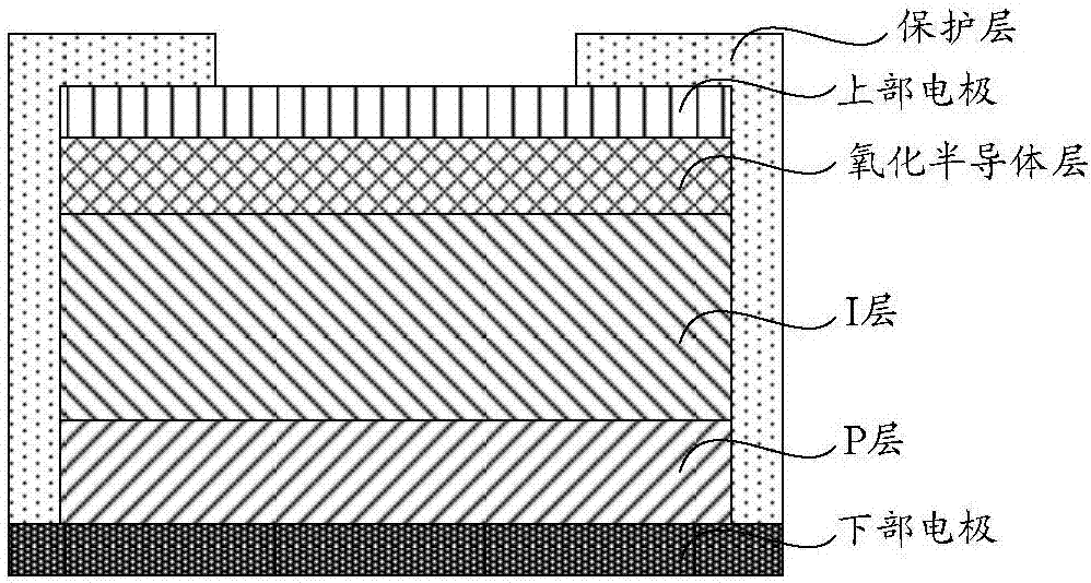
[0039] figure 1 It is a schematic structural diagram of an embodiment of a PIN unit device in this application, such as figure 1 As shown, the PIN device of the present invention includes: a lower electrode, a p-type heavily doped and intrinsic layer, that is, a PI layer, an oxide semiconductor layer, an upper electrode, and a protective layer. in,

[0040] The oxide semiconductor may be: for example, Indium Gallium Zinc Oxide (IGZO, Indium Gallium Zinc Oxide) and the like.

[0041] In the PIN unit device of the present invention, the oxide semiconductor is used to replace...


PUM


Abstract

The invention discloses a PIN unit device and a preparation method thereof, and a fingerprint recognition sensor and a preparation method thereof. The PIN unit device provided by the invention comprises a lower electrode, a PI layer, an oxide semiconductor layer, an upper electrode, and a protective layer. The oxide semiconductor layer can be indium gallium zinc oxide (IGZO) or the like. According to the PIN unit device of the invention, an oxide semiconductor instead of A-Si is used as an N+ layer. The oxide semiconductor, such as IGZO, has a wide band gap, and is completely transparent to visible light. Therefore, more light can reach an intrinsic layer, and the light response characteristic of the PIN device is improved.

Description

technical field [0001] The invention relates to but not limited to electronic technology, especially a PIN unit device and its preparation method, a fingerprint identification sensor and its preparation method. Background technique [0002] PIN photodetection device is the core electronic component of optical fingerprint recognition and X-Ray flat panel detector, and its photoelectric characteristics directly restrict the performance of the whole system. And its preparation method has restricted the level of product production efficiency again. [0003] In the preparation process of the PIN unit device, the n-type heavily doped layer, that is, the N+ layer, is formed by amorphous silicon (A-Si). Due to the narrow band gap of A-Si, it is not completely transparent to visible light and cannot allow more visible light. reaches the layer, thereby reducing the photoresponse characteristics of the PIN device. Contents of the invention [0004] The invention provides a PIN unit...

Claims


Application Information

Patent Timeline
Patent Type & Authority Applications(China)
IPC IPC(8): H01L27/144H01L31/032H01L31/105H01L31/18G06K9/00
CPCH01L27/1443H01L31/032H01L31/105H01L31/18G06V40/1318Y02P70/50
Inventor 孙建明李东升任庆荣
Owner BOE TECH GRP CO LTD
Learn More