cmos image sensor

An image sensor and pixel signal technology, which is used in image communication, TV, color TV components and other directions, and can solve the problems of large readout circuit area, difficulty in realizing column readout circuit layout, and inability to adjust.

Active Publication Date: 2020-10-20
INST OF SEMICONDUCTORS - CHINESE ACAD OF SCI
View PDF6 Cites 0 Cited by
  • Summary
  • Abstract
  • Description
  • Claims
  • Application Information

AI Technical Summary

Problems solved by technology

[0002] There is a compromise between the imaging frame rate and imaging resolution of CMOS (Complementary Metal Oxide Semiconductor) image sensors. Usually, once a CMOS image sensor is produced, the highest imaging frame rate and maximum resolution are determined and cannot be adjusted.
In addition, high-speed CMOS image sensors mostly adopt a column-parallel readout structure, each column is equipped with a readout circuit, so the area of ​​the readout circuit is relatively large, and at the same time, the layout of the column readout circuit is implemented in a narrow strip space (usually micron level). bring difficulties

Method used


Image

  • cmos image sensor
  • cmos image sensor
  • cmos image sensor

Examples


Embodiment

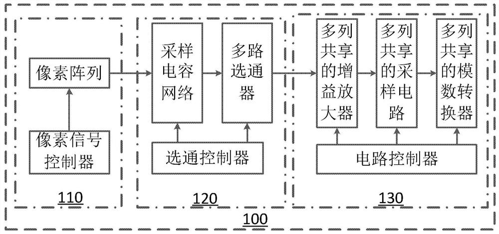
[0068] like figure 1 As shown, this embodiment proposes a CMOS image sensor 100, including:

[0069] A pixel signal generation module 110, configured to generate at least two pixel signals in different modes based on the timing control signal;

[0070] The pixel signal acquisition module 120 is used for collecting and storing pixel signals of different modes in a pipeline, and is also used for correlated double sampling of pixel signals of different modes;

[0071] The pixel signal processing module 130 is configured to perform multi-column sharing processing on correlated double-sampled pixel signals to obtain digital codes.

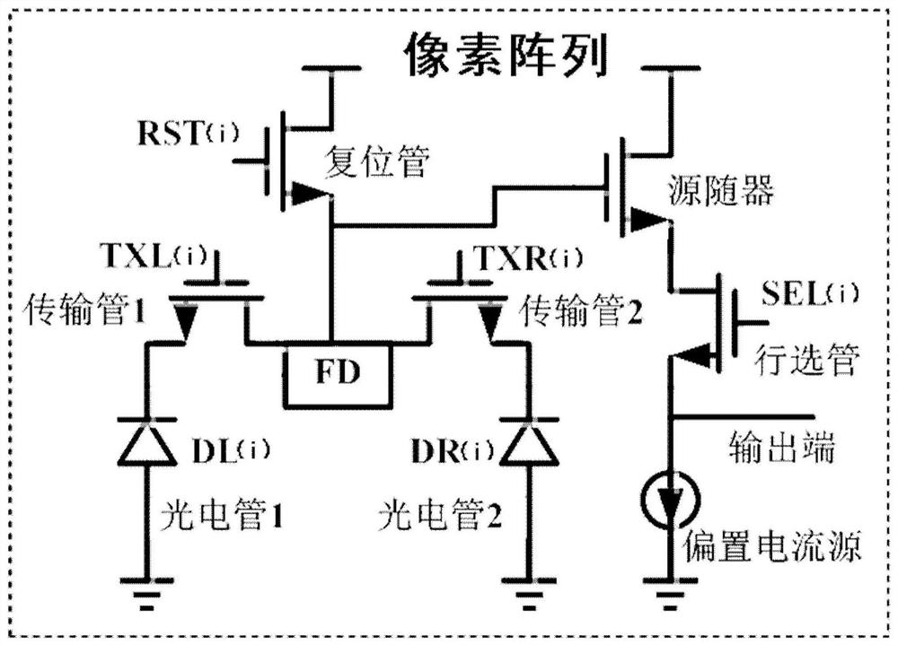
[0072] Specifically, the pixel signal generating module 110 includes a pixel signal controller and a pixel array, and the structure of the pixel array is as follows figure 2 shown. The pixel array consists of two symmetrical buried layer photodiodes DL(i) and DR(i), two symmetrical transmission transistors TXL(i) and TXR(i), a reset transistor RST(i...


PUM


Abstract

A CMOS image sensor and a video camera and a digital camera using the same, the sensor includes: a pixel signal generation module, which is used to generate pixel signals of different modes based on a timing control signal; a pixel signal acquisition module, which is used to collect and store different modes in a pipeline The pixel signal of the correlation double sampling is used for pixel signals of different modes; the pixel signal processing module is used for performing multi-column sharing processing on the pixel signal of correlation double sampling to obtain a digital code. Because the pixel signal generating module of the present invention can obtain pixel signals of different modes by adjusting the timing control signal of the pixel signal controller, the resolution and frame rate of the CMOS image sensor of the present invention are adjustable. The pixel signal sampling module and the pixel signal processing module can process pixel signals shared by multiple columns, so the circuit structure can process multi-column pixel signals in a compact and high-speed manner, reduce the chip area, effectively reduce the area of ​​the analog readout circuit, and make the layout easier to implement.

Description

technical field [0001] The invention belongs to the technical field of integrated circuits, and more specifically relates to a CMOS image sensor. Background technique [0002] There is a compromise between the imaging frame rate and imaging resolution of a CMOS (Complementary Metal Oxide Semiconductor) image sensor. Usually, once a CMOS image sensor is produced, its highest imaging frame rate and maximum resolution are determined and cannot be adjusted. In addition, high-speed CMOS image sensors mostly adopt a column-parallel readout structure, each column is equipped with a readout circuit, so the area of ​​the readout circuit is relatively large, and at the same time, the layout of the column readout circuit is implemented in a narrow strip space (usually micron level). bring difficulty. Contents of the invention [0003] Based on the above problems, the main purpose of the present invention is to provide a CMOS image sensor for solving at least one of the above technic...

Claims


Application Information

Patent Timeline
Patent Type & Authority Patents(China)
IPC IPC(8): H04N5/374H04N5/3745
CPCH04N25/76H04N25/77
Inventor 郭志强刘力源吴南健
Owner INST OF SEMICONDUCTORS - CHINESE ACAD OF SCI
Why Eureka
Try Eureka