High density flexible substrate manufacturing method

A technology of flexible substrates and manufacturing methods, which is applied in printed circuit manufacturing, flexible printed circuit boards, photolithography/patterning, etc., can solve the problem that the line width cannot be made small, and achieve the goals of saving time, reducing part of the process, and improving efficiency Effect

Active Publication Date: 2017-08-11
NAT CENT FOR ADVANCED PACKAGING
View PDF6 Cites 6 Cited by
  • Summary
  • Abstract
  • Description
  • Claims
  • Application Information

AI Technical Summary

Problems solved by technology

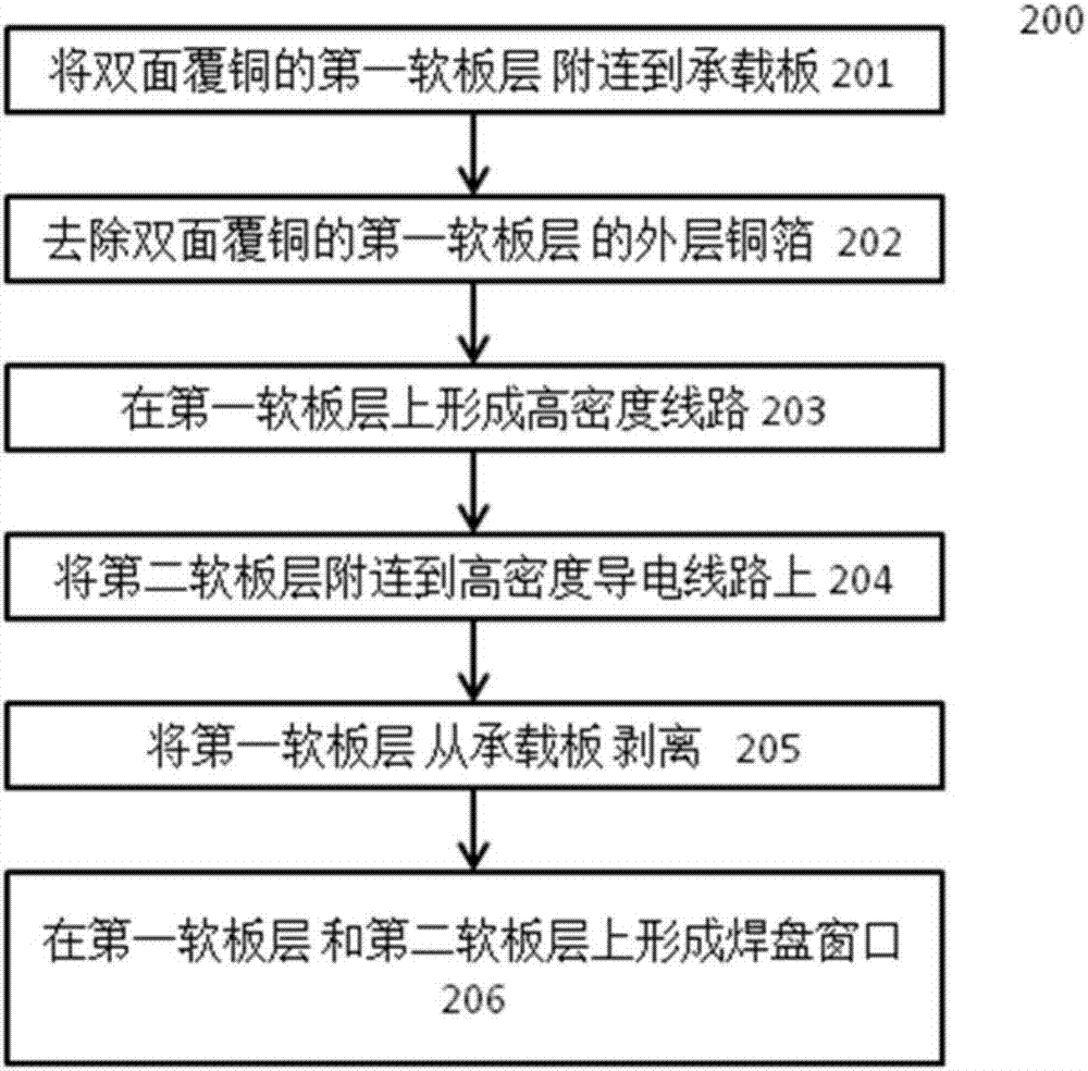
[0007] Aiming at the technical problems existing in the prior art that the line width cannot be made small when the line thickness is guaranteed to be certain, the embodiment of the present invention provides a high-density flexible substrate manufacturing method, including: removing the first flexible board with copper clad on both sides layer of the first layer of copper foil to expose the first surface of the first soft board layer; form a conductive line on the first surface of the first soft board layer; attach the second soft board layer to the On the conductive line; removing the second layer of copper foil of the first soft board layer; and forming at least one pad window on the first soft board layer and the second soft board layer so as to expose the pad

Method used


Image

  • High density flexible substrate manufacturing method
  • High density flexible substrate manufacturing method
  • High density flexible substrate manufacturing method

Examples


Embodiment Construction

[0024] In the following description, the present invention is described with reference to various examples. One skilled in the art will recognize, however, that the various embodiments may be practiced without one or more of the specific details, or with other alternative and / or additional methods, materials, or components. In other instances, well-known structures, materials, or operations are not shown or described in detail so as not to obscure aspects of the various embodiments of the invention. Similarly, for purposes of explanation, specific quantities, materials and configurations are set forth in order to provide a thorough understanding of embodiments of the invention. However, the invention may be practiced without these specific details. Furthermore, it should be understood that the various embodiments shown in the drawings are illustrative representations and are not necessarily drawn to scale.

[0025] In this specification, reference to "one embodiment" or "the...


PUM


Abstract

The invention provides a high density flexible substrate manufacturing method. The high density flexible substrate manufacturing method comprises steps that a first copper foil layer of a double-sided copper-clad first flexible printed circuit board layer is removed, and the first surface of the first flexible printed circuit board layer is exposed; a conductive line is formed on the first surface of the first flexible printed circuit board layer; a second flexible printed circuit board layer is connected with the conductive line in an attached manner; the second copper foil layer of the first flexible printed circuit board is removed; and at least one bonding pad window is formed in the first flexible printed circuit board layer and the second flexible printed circuit board layer to expose a bonding pad.

Description

technical field [0001] The invention relates to the field of semiconductor packaging, in particular to a method for manufacturing a high-density flexible substrate. Background technique [0002] Flexible substrates are circuit substrates made of flexible insulating substrates, which have many advantages that rigid substrates do not have. For example, it can be bent, wound, and folded freely, and can be arranged arbitrarily according to the requirements of space layout, and can be moved and stretched arbitrarily in three-dimensional space, so as to achieve the integration of component assembly and wire connection. Therefore, compared with ordinary circuit substrates, flexible substrates have huge performance and market advantages in electronic products such as wearable electronic devices and medical electronic devices that need to meet functions such as bending, winding, and folding. [0003] In the prior art, the surface circuit processing of flexible substrates generally a...

Claims


Application Information

Patent Timeline
Patent Type & Authority Applications(China)
IPC IPC(8): H05K3/10
CPCH05K3/108H05K2201/05H05K2203/0502
Inventor 于中尧
Owner NAT CENT FOR ADVANCED PACKAGING
Why Eureka
Try Eureka