Ion implantation apparatus

一种离子注入装置、离子注入的技术,应用在放电管、电气元件、半导体/固态器件制造等方向,能够解决降低离子注入处理生产率等问题

Active Publication Date: 2017-08-18
SUMITOMO HEAVY IND ION TECH
View PDF9 Cites 5 Cited by
  • Summary
  • Abstract
  • Description
  • Claims
  • Application Information

AI Technical Summary

Problems solved by technology

Usually, the beam setting process takes tens of seconds to several minutes, so if the beam setting process must be performed every time the rotation angle of the wafer is changed, the productivity of the ion implantation process will be greatly reduced

Method used


Image

  • Ion implantation apparatus
  • Ion implantation apparatus
  • Ion implantation apparatus

Examples


Embodiment Construction

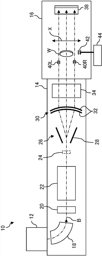
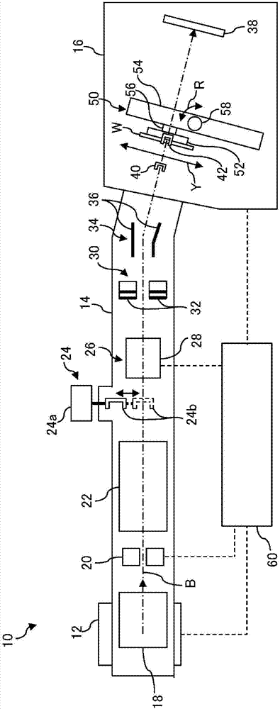
[0033] Hereinafter, modes for implementing the present invention will be described in detail with reference to the drawings. In addition, in the description of the drawings, the same reference numerals are assigned to the same elements, and overlapping descriptions are appropriately omitted. In addition, the structures described below are examples and do not limit the scope of the present invention in any way.

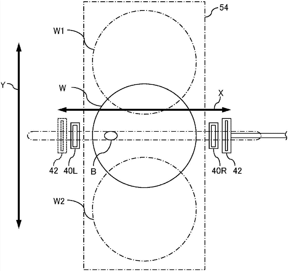
[0034] Before describing the embodiment, the outline of the present invention will be described. This embodiment is an ion implantation apparatus for continuously performing a plurality of ion implantation steps with different implantation conditions on the same wafer. The ion implantation apparatus includes: a beam scanner for reciprocatingly scanning the ion beam in a predetermined scanning direction; a measuring instrument for measuring the beam current density distribution in the scanning direction of the reciprocatingly scanned ion beam; The scanned ion beam is ...


PUM


Abstract

The invention provides an ion implantation apparatus which can guarantee both the production rate of ion implantation treatment and the uneven injection precision in wafer surfaces. The ion implantation apparatus (10) performs a plurality of ion implantation processes having different implantation conditions to a same wafer successively. The plurality of ion implantation processes are: (a) provided so that twist angles of the wafer differ from each other; (b) configured so that an ion beam is irradiated to a wafer surface to be processed that moves in a reciprocating movement direction; and (c) provided so that a target value of a beam current density distribution of the ion beam is variable in accordance with a position of the wafer in the reciprocating movement direction. Before performing the plurality of ion implantation processes to the same wafer successively, a control device executes a setup process in which a plurality of scanning parameters corresponding to the respective implantation conditions of the plurality of ion implantation processes are determined collectively.

Description

technical field [0001] This application claims priority based on Japanese Patent Application No. 2015-193965 filed in Japan on September 30, 2015. The entire contents of this Japanese application are incorporated herein by reference. [0002] The present invention relates to an ion implantation device, and relates to an ion implantation device for continuously performing a plurality of ion implantation processes on the same wafer. Background technique [0003] In the semiconductor manufacturing process, a process of implanting ions into a semiconductor wafer (hereinafter also referred to as "ion implantation process") is routinely performed for the purpose of changing the conductivity of the semiconductor, changing the crystal structure of the semiconductor, and the like. The device used in the ion implantation process is called an ion implantation device, which has the function of generating ions from the ion source and accelerating the generated ions to form an ion beam, ...

Claims


Application Information

Patent Timeline
Patent Type & Authority Applications(China)
IPC IPC(8): H01J37/20H01J37/302H01J37/317H01L21/67H01L21/687
CPCH01J37/20H01J37/3023H01J37/3171H01L21/67011H01L21/68764H01J2237/31701H01J2237/20221H01J2237/20214H01J2237/20207H01L21/26586H01J37/304H01J2237/31703H01J2237/30483H01J2237/20228H01L21/265
Inventor 二宫史郎冈本泰治越智昭浩上野勇介
Owner SUMITOMO HEAVY IND ION TECH
Why Eureka
Try Eureka