A junctionless field effect transistor

A field effect transistor, junctionless technology, applied in semiconductor devices, electrical components, circuits, etc., can solve problems such as poor stability

Active Publication Date: 2020-04-14
PEKING UNIV SHENZHEN GRADUATE SCHOOL
View PDF8 Cites 3 Cited by
  • Summary
  • Abstract
  • Description
  • Claims
  • Application Information

AI Technical Summary

Problems solved by technology

[0004] The present application provides a junctionless field effect transistor to solve the problem of poor stability of junctionless field effect transistors in the prior art

Method used


Image

  • A junctionless field effect transistor
  • A junctionless field effect transistor
  • A junctionless field effect transistor

Examples


Embodiment 1

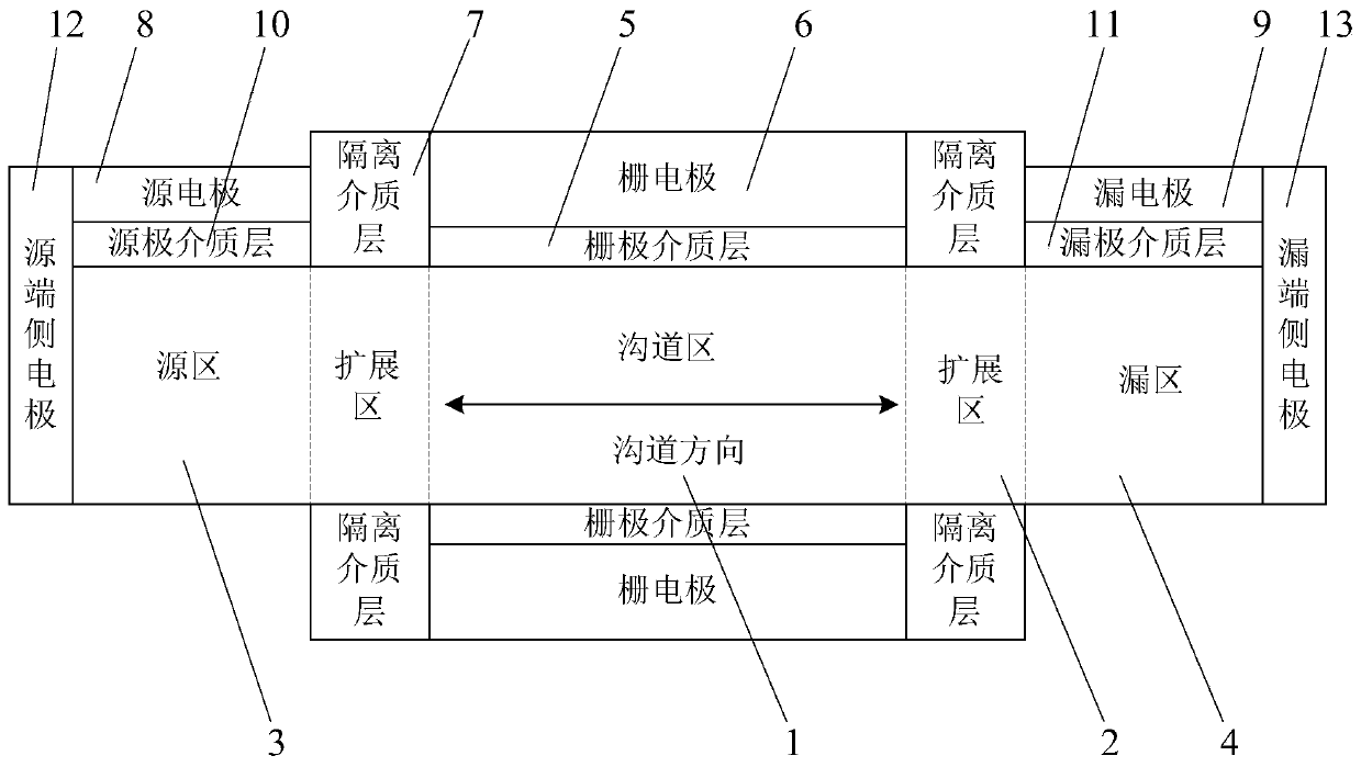
[0040] Please refer to figure 1 , Is a schematic structural diagram of a junctionless field effect transistor provided by an embodiment of the present invention, such as figure 1 As shown, the junctionless field effect transistor includes a channel region 1, a source region 3, a drain region 4, a gate electrode 6, a source electrode 8 and a drain electrode 9.

[0041] Among them, the source region 3 and the drain region 4 are centered symmetrically on both sides of the channel region 1, so that the carriers in the channel region 1 can travel from the source region 3 to the drain region 4 or from the drain region 4 to the source region 3. The direction in which the source region 3 and the drain region 4 are arranged can be understood as the channel direction to indicate the direction of carrier transport; in an exemplary embodiment, the source region 3 and the channel region 1 can also be An extension area 2 is provided, and an extension area 2 can also be provided between the drai...

Embodiment 2

[0065] On the basis of Example 1, please refer to figure 1 with Figure 5 , Is a schematic structural diagram of a tri-gate junctionless field effect transistor provided by an embodiment of the present invention. Such as Figure 5 As shown, the junctionless field effect transistor includes a channel region 1, an extension region 2, a source region 3, and a drain region 4; wherein, the channel region 1, the extension region 2, the source region 3 and the drain region 4 all include top Surface and two side surfaces, and the channel region 1, the extension region 2, the source region 3 and the drain region 4 are all arranged on the substrate 12, which can be a silicon substrate, etc., which is not limited in the embodiment of the present invention; The gate dielectric layer covers the top surface and all sides of the channel region 1, and the gate electrode 6 covers the gate dielectric layer to form a three-gate structure, thereby enhancing the control ability of the gate electrode...

Embodiment 3

[0068] On the basis of Example 1, please refer to figure 1 with Image 6 , Is a schematic diagram of the structure of a ring-gate junctionless field effect transistor provided by an embodiment of the present invention, such as Image 6 As shown, the junctionless field effect transistor includes a channel region, an extension region, a source region, and a drain region; wherein the channel region, the extension region, the source region and the drain region are all cylindrical structures; the gate dielectric layer is arranged around On the outer circumference of the channel region, the gate electrode 6 is further arranged around the outer circumference of the gate dielectric layer to form a ring-gate structure; the isolation dielectric layer 7 is arranged around the outer circumference of the extension area, thereby realizing the gap between the source electrode 8 and the gate electrode 6, And the isolation between the drain electrode 9 and the gate electrode 6; the source diele...


PUM

PropertyMeasurementUnit
thicknessaaaaaaaaaa
thicknessaaaaaaaaaa
thicknessaaaaaaaaaa

Abstract

The invention provides a non-junction field-effect transistor. The non-junction field-effect transistor includes a source region and a drain region, wherein the source region and the drain region are arranged at two sides of a channel region in a central symmetry manner; the channel region, the source region and the drain region are the same in the doping type and the doping concentration; the channel region is provided with a gate dielectric layer and a gate electrode which is arranged on the gate dielectric layer; the source region and the drain region are respectively provided with a source electrode dielectric layer, a source electrode, a source end side electrode, a drain electrode dielectric layer, a drain electrode and a drain end side electrode; isolating dielectric layers isolate the source electrode from the gate electrode; and the work functions of the source electrode and the drain electrode are the work functions which are determined according to the doping type so as to form a conductive carrier layer on the surface of the source region and the surface of the drain region. The non-junction field-effect transistor can accumulate the corresponding type of carriers on the source region and the drain region to perform current transportation by adjusting the metal work functions of the source electrode and the drain electrode. The structure of the non-junction field-effect transistor can restrain the influence of rough edge of a technological fluctuation line on the device performance, can maintain the current driving capability of a non-junction device, and can optimize the subthreshold feature of the non-junction device so as to improve the stability of device.

Description

Technical field [0001] This application relates to the technical field of semiconductor integrated circuit devices, in particular to a junctionless field effect transistor. Background technique [0002] Under the guidance of Moore's Law in the integrated circuit industry, device sizes are getting smaller and smaller. However, as the size of the device continues to shrink, the performance of the device is increasingly affected by effects such as threshold voltage drift and increase in leakage current. Therefore, a variety of new device structures have been proposed to improve the gate control ability to suppress short channel defects. effect. However, with the further reduction of devices, especially after the device size is reduced to sub-10 nanometers in the next few years, the precision control of doping becomes extremely important and challenging; on the one hand, the control precision of the channel atom doping number needs to reach The units position avoids large fluctuati...

Claims


Application Information

Patent Timeline
Patent Type & Authority Patents(China)
IPC IPC(8): H01L29/06H01L29/08H01L29/10H01L29/78
CPCH01L29/0657H01L29/0847H01L29/1079H01L29/78
Inventor 万文波楼海君肖颖林信南
Owner PEKING UNIV SHENZHEN GRADUATE SCHOOL
Why Eureka
Try Eureka