Transverse structure germanium/silicon heterojunction avalanche photoelectric detector and preparation method thereof

A silicon heterojunction, avalanche photoelectric technology, applied in photovoltaic power generation, circuits, electrical components and other directions, can solve the problems of difficult preparation, high control requirements for doping, complex structure of avalanche photodetectors, etc., and achieves easy preparation. , good consistency and simple structure

Active Publication Date: 2017-08-18
INST OF SEMICONDUCTORS - CHINESE ACAD OF SCI +1
View PDF7 Cites 12 Cited by
  • Summary
  • Abstract
  • Description
  • Claims
  • Application Information

AI Technical Summary

Problems solved by technology

[0003] However, the structure of this avalanche photodetector is complex, especially the requirements for doping control are very high, and the preparation is relatively difficult.

Method used


Image

  • Transverse structure germanium/silicon heterojunction avalanche photoelectric detector and preparation method thereof
  • Transverse structure germanium/silicon heterojunction avalanche photoelectric detector and preparation method thereof
  • Transverse structure germanium/silicon heterojunction avalanche photoelectric detector and preparation method thereof

Examples


Embodiment 1

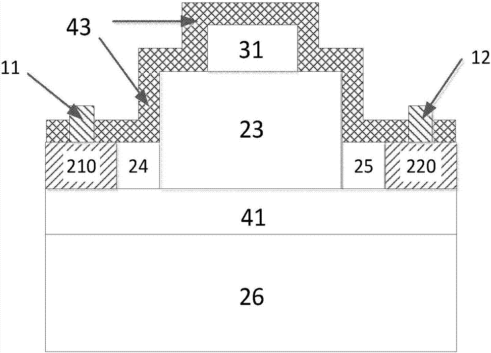
[0045] Example 1 as figure 1 Shown is a lateral structure germanium / silicon heterojunction avalanche photodetector provided by an embodiment of the present invention, including: a positive electrode 11, a negative electrode 12, a silicon P + Contact region 210, silicon N + Contact region 220 , silicon mesa region 23 , first silicon space region 24 , second silicon space region 25 , germanium epitaxial layer 31 , surface passivation layer 43 , buried silicon oxide 41 and silicon substrate 26 .

[0046] The silicon substrate 26 and the buried silicon oxide 41 are made of SOI material, and the buried silicon oxide 41 is formed on the silicon substrate 26 . The silicon mesa region 23 is formed on the buried silicon oxide 41 by etching the surface device silicon layer on the buried silicon oxide 41 .

[0047] The first silicon space region 24 and the second silicon space region 25 are respectively formed on the buried silicon oxide 41 on both sides of the silicon mesa region 23 ,...

Embodiment 2

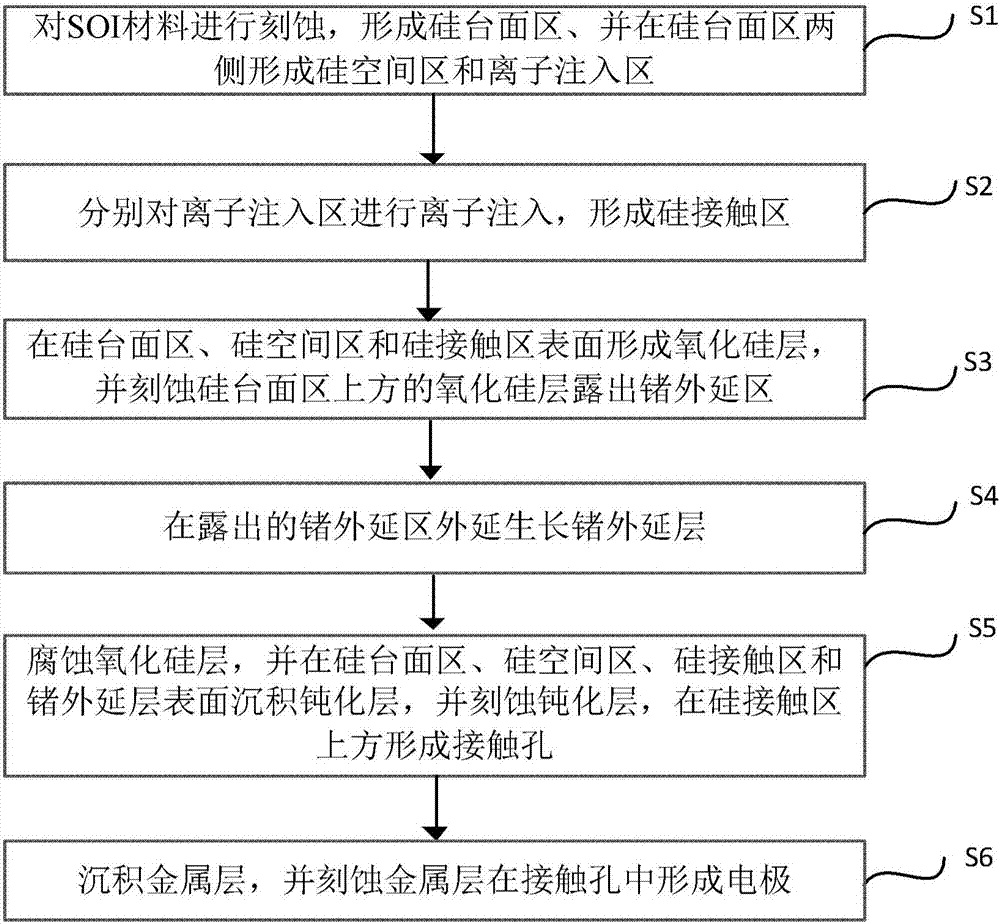
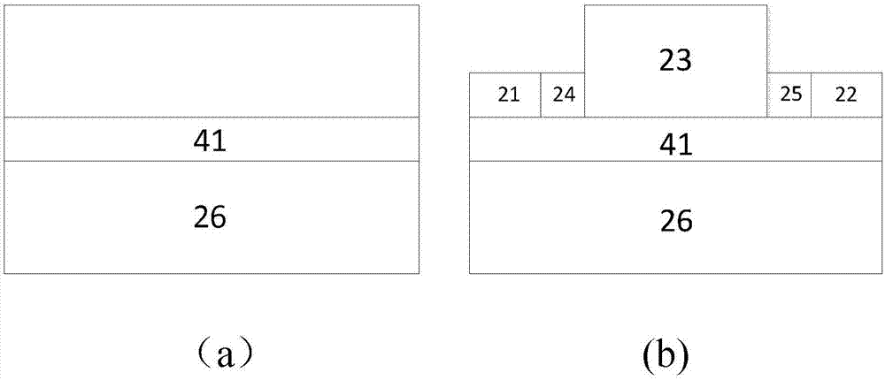
[0057] figure 2 The flow chart of the steps of a method for preparing a lateral structure germanium / silicon heterojunction avalanche photodetector provided by the patent embodiment of the present invention, image 3 A schematic diagram of the structure during device fabrication is given, corresponding to the following implementation steps. Combine below figure 2 and image 3 Introduce the preparation method of the device:

[0058] Step S1: Etching the SOI material to form a silicon mesa region, and forming silicon space regions and ion implantation regions on both sides of the silicon mesa region.

[0059] Such as image 3 As shown in (a), the preparation starts from the SOI material, which has a three-layer structure, including a stacked substrate 26 , buried silicon oxide 41 , and a surface device silicon layer above the buried silicon oxide 41 .

[0060] First, the SOI material is cleaned by organic and inorganic solvents. If the SOI material has a good clean packag...


PUM


Abstract

The invention discloses a transverse structure germanium / silicon heterojunction avalanche photoelectric detector which is prepared on an SOI (Silicon-on-Insulator) substrate and has a double-tabletop structure. The transverse structure germanium / silicon heterojunction avalanche photoelectric detector comprises a substrate, a buried silicon oxide layer, a silicon tabletop area, silicon space areas, silicon contact areas, electrodes and a germanium epitaxial layer. The buried silicon oxide layer is formed on the silicon substrate. The silicon tabletop area is formed on the buried silicon oxide layer. The silicon space areas are formed on the buried silicon oxide layer at two sides of the silicon tabletop area. The silicon contact areas are formed on the buried silicon oxide layer outside the silicon space areas. The germanium epitaxial layer is formed on the silicon tabletop area. The electrodes are in ohmic contact with the silicon contact areas. The two electrodes are manufactured on a silicon layer. A germanium light absorbing layer is arranged above the silicon layer. A bias voltage which is applied to the two electrodes realize electric fields with different strengths in the light absorbing layer and the silicon layer. Light absorption is realized in the germanium and an avalanche multiplication process is realized in the silicon layer.

Description

technical field [0001] The invention relates to the field of semiconductor photodetectors, in particular to a lateral structure germanium / silicon heterojunction avalanche photodetector and a preparation method thereof. Background technique [0002] Avalanche photodetector is a photodetector with photoresponse multiplication function, which is especially suitable for detecting weak light signals. The basic principle is that light is absorbed by the detector to generate photogenerated carriers. Under the action of an electric field, electrons and holes gain energy and accelerate their movement. When the electric field is strong enough, electrons and holes are realized through collision ionization in motion. The multiplied, multiplied electrons and holes are collected by the electrodes, so as to obtain a multiplied and amplified response current. Although the multiplication of the photogenerated current is obtained, a large multiplication excess noise will be generated at the ...

Claims


Application Information

Patent Timeline
Patent Type & Authority Applications(China)
IPC IPC(8): H01L31/028H01L31/107H01L31/18
CPCH01L31/028H01L31/1075H01L31/1804Y02E10/547
Inventor 成步文刘智武文周薛春来李传波张华
Owner INST OF SEMICONDUCTORS - CHINESE ACAD OF SCI
Why Eureka
Try Eureka