Fan-out single die packaging structure, and preparation method thereof

A packaging structure, fan-out technology, applied in semiconductor/solid-state device manufacturing, electrical components, electric solid-state devices, etc., can solve the problem of high manufacturing cost of fan-out wafer-level packaging technology, to prevent position shifting, shorten Process time, effect of quality assurance

Inactive Publication Date: 2017-08-29
SJ SEMICON JIANGYIN CORP
View PDF5 Cites 17 Cited by
  • Summary
  • Abstract
  • Description
  • Claims
  • Application Information

AI Technical Summary

Problems solved by technology

[0006] In view of the shortcomings of the prior art described above, the purpose of the present invention is to provide a fan-out single-die packaging structure and its preparation method, which is used to solve the problem of high manufacturing cost of the existing fan-out wafer-level packaging process

Method used


Image

  • Fan-out single die packaging structure, and preparation method thereof
  • Fan-out single die packaging structure, and preparation method thereof
  • Fan-out single die packaging structure, and preparation method thereof

Examples


Embodiment 1

[0071] like Figure 1 to Figure 11 As shown, this embodiment provides a method for preparing a fan-out single-die packaging structure, and the method includes:

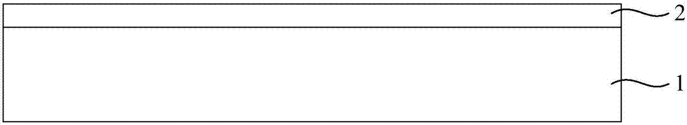
[0072] 1) Provide a carrier 1, and form an adhesive layer 2 on the upper surface of the carrier 1;

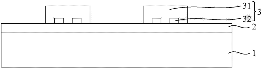
[0073] 2) forming a chip structure 3 on the upper surface of the adhesive layer 2, the chip structure 3 includes a bare chip 31 and a contact pad 32 located on the bare chip 31 and electrically connected to the bare chip 31;

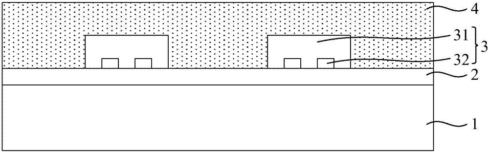
[0074] 3) forming a plastic sealing layer 4 on the upper surface of the adhesive layer 2, and the plastic sealing layer 4 covers the chip structure 3;

[0075] 4) removing the carrier 1 and the adhesive layer 2 to expose the chip structure 3;

[0076] 5) Form a first dielectric layer 5 on the surface of the plastic encapsulation layer 4 exposing the chip structure 3, and perform photoetching on the first dielectric layer 5 to form a first dielectric layer 5 exposing the contact pad 32. opening...

Embodiment 2

[0120] Such as Figure 11 As shown, this embodiment provides a fan-out single die packaging structure, the packaging structure includes:

[0121] A chip structure 3, the chip structure 3 comprising a bare chip 31 and a contact pad 32 located on the bare chip 31 and electrically connected to the bare chip 31;

[0122] enclosing the chip structure 3 while exposing the plastic encapsulation layer 4 on the surface where the contact pad 32 is located;

[0123] The first dielectric layer 5 located on the upper surface of the plastic encapsulation layer 4 and the chip structure 3, the first dielectric layer 5 exposes the contact pad 32 through the first opening 6;

[0124] A rewiring layer 7 located on the upper surface of the first dielectric layer 5 and the contact pad 32, the rewiring layer 7 exposes the first dielectric layer 5 through the second opening 8;

[0125] The second dielectric layer 9 located on the upper surface of the rewiring layer 7 and the first dielectric layer...


PUM


Abstract

The invention provides a fan-out single die packaging structure, and a preparation method thereof. The preparation method comprises the following steps: a carrier is provided, and a bonding layer is formed on the carrier; chip structures are formed on the bonding layer; a plastic packaging layer is formed on the bonding layer, wherein the chip structures are coated by the plastic packaging layer; the carrier and the bonding layer are removed to expose the chip structures; a first dielectric layer is formed on the plastic packaging layer with the exposed chip structures, and photoetching is carried out on the first dielectric layer to form first openings through which contact pads are exposed; a redistribution layer is formed on the first dielectric layer and the contact pads, and photoetching is carried out on the redistribution layer to form second openings through which the first dielectric layer is exposed; a second dielectric layer is formed on the redistribution layer and the first dielectric layer, and laser etching is carried out on the second dielectric layer to form third openings through which the redistribution layer is exposed; and welded ball bumps are formed on the third openings. The fan-out single die packaging structure and the preparation method thereof provided by the invention have the advantage that the problem of high manufacturing cost of the conventional fan-out packaging process is solved.

Description

technical field [0001] The invention relates to the technical field of semiconductor packaging, in particular to a fan-out single-die packaging structure and a preparation method thereof. Background technique [0002] Lower cost, more reliable, faster and higher density circuits are the goals pursued by integrated circuit packaging. In the future, integrated circuit packaging will increase the integration density of various electronic components by continuously reducing the minimum feature size. Currently, advanced packaging methods include: Wafer Level Chip Scale Packaging (WLCSP), Fan-Out Wafer Level Package (FOWLP), Flip Chip, Package on Package (Package on Package, POP) and so on. [0003] Fan-out wafer-level packaging is an embedded chip packaging method for wafer-level processing. It is currently one of the advanced packaging methods with more input / output ports (I / O) and better integration flexibility. Compared with conventional wafer-level packaging, fan-out wafer...

Claims


Application Information

Patent Timeline
Patent Type & Authority Applications(China)
IPC IPC(8): H01L21/60H01L23/488
CPCH01L24/11H01L24/13H01L24/83H01L2224/0231H01L2224/02331H01L2224/02379H01L2224/02381H01L2224/13024H01L2224/11019H01L2224/83005H01L2224/96H01L2224/04105H01L2224/12105
Inventor 陈彦亨林正忠何志宏
Owner SJ SEMICON JIANGYIN CORP
Why Eureka
Try Eureka