

A method for arranging semiconductor wafers to improve chip yield
A technology of semiconductor and wafer yield, applied in the direction of semiconductor devices, semiconductor/solid-state device components, semiconductor/solid-state device testing/measurement, etc. The effect of block area
- Summary
- Abstract
- Description
- Claims
- Application Information
AI Technical Summary
Problems solved by technology
Method used
Image

Examples
Embodiment Construction
[0021] The following will clearly and completely describe the technical solutions in the embodiments of the present invention. Obviously, the described embodiments are only some of the embodiments of the present invention, rather than all the embodiments. Based on the embodiments of the present invention, all other embodiments obtained by persons of ordinary skill in the art without making creative efforts belong to the protection scope of the present invention.
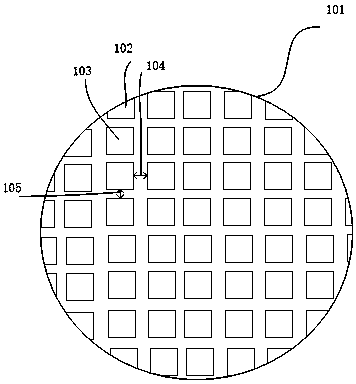
[0022] figure 1 It is a layout diagram of a chip on a semiconductor wafer. 101 is a semiconductor wafer, its shape is circular, and now it is generally divided into 6-inch (about 150mm in diameter) wafer, 8-inch (about 200mm in diameter) wafer, and 12-inch (300mm) wafer. A wafer is generally filled with identical or different chips in chip manufacturing. figure 1 Is full of chips of the same size. Since chips are generally rectangular, chips 102 with incomplete borders, except for chips with incomplete borders, ar...
PUM
 Abstract
Description
Claims
Application Information