Unlock instant, AI-driven research and patent intelligence for your innovation.

Single photon avalanche photodiode time delay integration CMOS image sensor

A time delay integration and photodiode technology, which is applied in the field of time delay integration CMOS image sensors, single photon avalanche photodiodes, and CMOS integrated circuits, can solve problems such as insufficient detection capability, achieve global exposure, low readout noise, low pressure effect

Inactive Publication Date: 2017-08-29
TIANJIN UNIV
View PDF6 Cites 8 Cited by
  • Summary
  • Abstract
  • Description
  • Claims
  • Application Information

AI Technical Summary

Problems solved by technology

[0004] In order to overcome the deficiencies of the prior art, the present invention aims at the problem of insufficient detection ability of ordinary TDI technology under low-light conditions, and uses SPAD as the pixel of the TDI image sensor to detect low-light conditions.

Method used


Image

  • Single photon avalanche photodiode time delay integration CMOS image sensor
  • Single photon avalanche photodiode time delay integration CMOS image sensor
  • Single photon avalanche photodiode time delay integration CMOS image sensor

Examples


Embodiment Construction

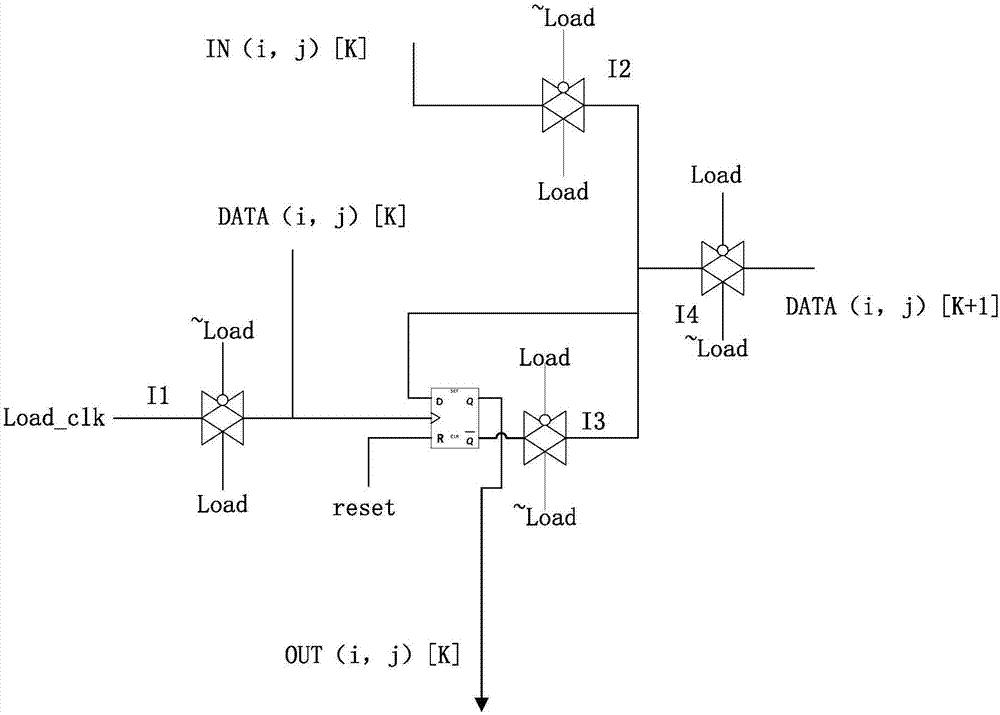
[0013] The system circuit structure diagram is as follows figure 1 As shown, the matrix of X multiplied by Y is formed by the arrangement of square pixels, and the internal circuit structure diagram of the i-th row and j-th column pixel is as follows figure 2 As shown, it is composed of SPAD unit and circuit unit. Taking N-bit output precision as an example, the SPAD unit is controlled by the select signal to convert the external signal source into a pulse signal. A pixel has N circuit units in total. Taking the Kth unit as an example, it is connected to IN(i, j)[k], OUT(i, j)[k], DATA(i, j)[k], DATA(i,j)[k+1] four signals, where OUT(i,j)[k]=IN(i+1,j)[k]. Its internal structure diagram is as follows Figure 4 shown. It is composed of D flip-flop and transmission gate with reset function. IN(i,j)[k] is connected to the input terminal of transmission gate I2, the output terminal of I2 is connected to the D terminal of the D flip-flop, DATA(i,j)[k] is connected to the clock ...


PUM


Abstract

The invention relates to the field of CMOS integrated circuits, aiming at solving the problem that an ordinary TDI technology has poor detection capabilities in low light conditions and achieving the purpose of taking an SPAD as the pixel of a TDI image sensor to detect lower illumination. And meanwhile, the invention also has the characteristics of global exposure, simple timing sequence design and the like. The technical scheme adopted by the invention is that a single photon avalanche photodiode time delay integration CMOS image sensor structurally comprises an X*Y matrix arranged by square pixels, wherein the internal circuit structure of the pixel at the i-th row and the j-th column consists of an SPAD unit and a circuit unit, and the SPAD unit is controlled by a select signal to convert an external signal source into a pulse signal; and one pixel totally includes N circuit units, and four signals are accessed to the k-th circuit unit. The single photon avalanche photodiode time delay integration CMOS image sensor disclosed by the invention is mainly applied to the occasions of designing and manufacturing CMOS integrated circuits.

Description

technical field [0001] The invention relates to the field of CMOS integrated circuits, in particular to the fields of time delay integration CMOS image sensors and single photon avalanche photodiodes. Background technique [0002] Solid-state image sensors are mainly divided into two types: Complementary Metal Oxide Semiconductor (CMOS) image sensors and Charged Coupled Device (CCD) image sensors. The CMOS image sensor has the advantages of low power consumption, small size, and high reliability because it can be embedded in a planar process. In the CMOS image sensor, according to the arrangement of pixels, it can be divided into two types: area array and line array. For the area array image sensor, a complete frame of two-dimensional image information can be obtained by one exposure, which is often used in monitoring, video recording, photography, etc., but its disadvantage is that the total number of pixels is large, and the pixels in each row are limited, so the frame ra...

Claims


Application Information

Patent Timeline
IPC IPC(8): H04N5/374H04N5/378H04N5/351
CPCH04N25/50H04N25/76H04N25/75
Inventor 徐江涛李炜韩立镪聂凯明史再峰高静
Owner TIANJIN UNIV