Waveguide micro-nano processing system and processing method
What is AI technical title?
AI technical title is built by Patsnap AI team. It summarizes the technical point description of the patent document.
A micro-nano processing and waveguide technology, which is applied in metal processing equipment, manufacturing tools, welding equipment, etc., can solve the problems of cumbersome processing steps, high processing costs, and high processing environment requirements, and achieves low processing environment requirements and processing method steps. Less, the effect of improving the processing environment
Active Publication Date: 2019-01-04
HUBEI UNIV OF TECH
View PDF8 Cites 0 Cited by
Summary
Abstract
Description
Claims
Application Information
AI Technical Summary
This helps you quickly interpret patents by identifying the three key elements:
Problems solved by technology
Method used
Benefits of technology
Problems solved by technology
At present, the production of optical waveguides mostly adopts methods such as chemical etching and ion etching. The above-mentioned methods have cumbersome processing steps, high requirements on the processing environment, and high processing costs.
Method used
Image
Click on the blue label to locate the original text in one second.
Reading with bidirectional positioning of images and text.
Examples
Embodiment Construction
[0019] The waveguide micro-nano processing system and processing method involved in the present invention will be described in detail below with reference to the accompanying drawings.
[0020]
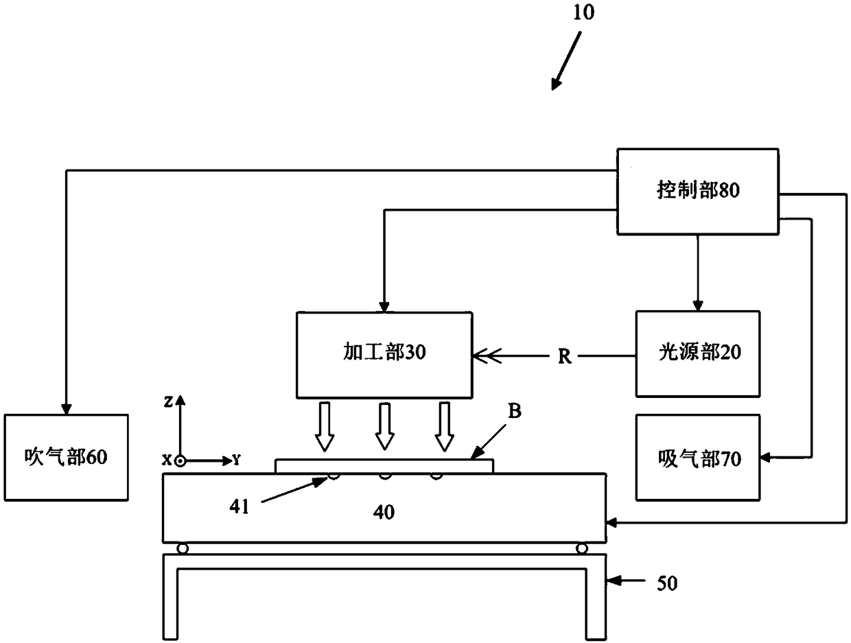
[0021] Such as figure 1 As shown, the waveguide micro-nano processing system 10 includes a light source unit 20 , a processing unit 30 , a multi-degree-of-freedom table 40 , an optical table 50 , an air blowing unit 60 , an air suction unit 70 and a control unit 80 .
[0022] The light source section 20 includes a laser, which is any one of nanosecond, picosecond, and femtosecond lasers, for supplying a laser beam.
[0023] The processing part 30 is arranged on the optical path of the light source part 20, and is used to focus the laser beam on the substrate B for photolithography processing, and monitor the processing process in real time. The substrate B used for processing can be materials such as silicon dioxide, silicon, and ceramics.
[0024] The multi-degree-of-freedom tabl...
PUM
Property
Measurement
Unit
thickness
aaaaa
aaaaa
thickness
aaaaa
aaaaa
Abstract
The invention provides a waveguide micro-nanometer machining system and method. The waveguide micro-nanometer machining system and method are low in machining cost, high in precision and good in consistency. The waveguide micro-nanometer machining system is characterized by, comprising, a light source portion, a machining portion, a multi-freedom-degree workbench, an optical platform, a blowing portion, a suction portion and a control portion, wherein the light source portion provides laser beams, the machining portion focuses the laser beams on a substrate for photolithography machining and monitors the machining process in real time, the machining portion is provided with a variable-focus lens, a three-dimensional morphology instrument, a camera and a temperature measuring instrument, the multi-freedom-degree workbench drives the substrate to move in multiple freedom degree directions according to a preset waveguide pattern, the optical platform is used for installation of the multi-freedom-degree workbench and isolates external vibration, the blowing portion is arranged on one side of the multi-freedom-degree workbench and conducts blowing towards a machining area, the suction portion is arranged on the other side of the multi-freedom-degree workbench and conducting suction and removal on the gas blown by the blowing portion, and the control portion is connected with the light source portion, the machining portion, the multi-freedom-degree workbench, the optical platform, the blowing portion and the suction portion and controls operation of the light source portion, the machining portion, the multi-freedom-degree workbench, the optical platform, the blowing portion and the suction portion.
Description
technical field [0001] The invention belongs to the field of micro-nano manufacturing and processing, and in particular relates to a waveguide micro-nano processing system and a corresponding processing method. technical background [0002] When the light wave is confined to propagate in the waveguide medium determined in the medium, the light wave channel formed by this medium is called an optical medium waveguide, or waveguide for short. At present, optical waveguides are mostly produced by chemical etching, ion etching and other methods. The above-mentioned methods have cumbersome processing steps, high requirements on the processing environment, and high processing costs. Contents of the invention [0003] The present invention is made to solve the above problems, and aims to provide a waveguide micro-nano processing system and processing method with low processing cost, high precision and good consistency. [0004] In order to achieve the above object, the present in...
Claims
Application Information
Patent Timeline
Application Date:The date an application was filed.
Publication Date:The date a patent or application was officially published.
First Publication Date:The earliest publication date of a patent with the same application number.
Issue Date:Publication date of the patent grant document.
PCT Entry Date:The Entry date of PCT National Phase.
Estimated Expiry Date:The statutory expiry date of a patent right according to the Patent Law, and it is the longest term of protection that the patent right can achieve without the termination of the patent right due to other reasons(Term extension factor has been taken into account ).
Invalid Date:Actual expiry date is based on effective date or publication date of legal transaction data of invalid patent.

