Routing common method for different impedance signal lines and PCB board

A PCB board and impedance signal technology, which is applied in the field of PCB wiring, can solve the problems of increasing PCB board production costs, affecting product efficiency and reliability, and reducing PCB board production yield, so as to reduce development costs and reduce high-speed wiring Quantity, size reduction area and effects of laminated layers

Inactive Publication Date: 2017-09-01
ZHENGZHOU YUNHAI INFORMATION TECH CO LTD
View PDF4 Cites 1 Cited by
  • Summary
  • Abstract
  • Description
  • Claims
  • Application Information

AI Technical Summary

Problems solved by technology

However, increasing the area of ​​the PCB board and the number of laminated layers will increase the production cost of the PCB board card. At the same time, the larger the area of ​​the board card and the increase in the number of layers will also increase the complexity of the PCB board factory's processing and reduce the cost of the PCB board. Board produc

Method used


Image

  • Routing common method for different impedance signal lines and PCB board
  • Routing common method for different impedance signal lines and PCB board
  • Routing common method for different impedance signal lines and PCB board

Examples


Example Embodiment

[0023] The present invention will be further described below in conjunction with the drawings and specific embodiments.

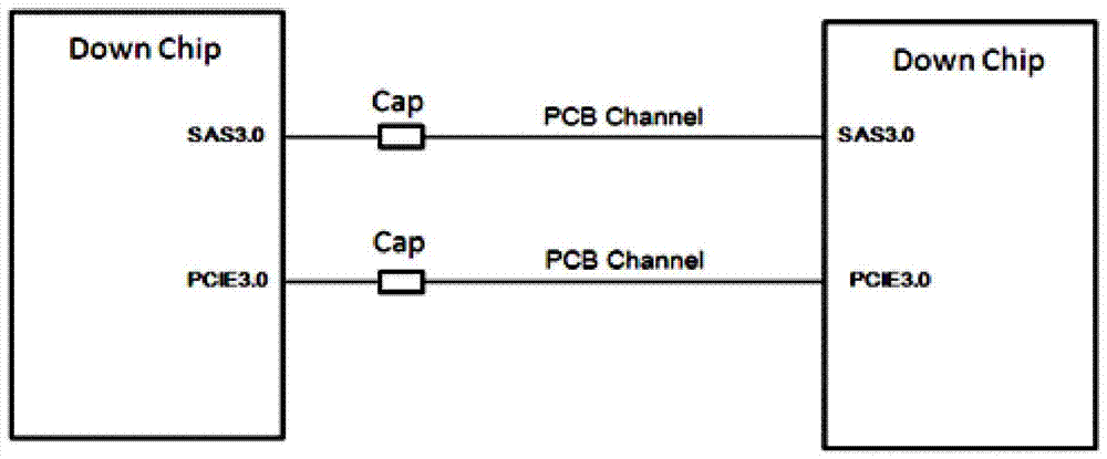
[0024] A method for realizing the sharing of different impedance signal lines. The process is to connect the signal lines with different impedance values ​​on the PCB board to the Cap capacitor, and then all the cap capacitors share the PCB Trace channel. The Cap The capacitor acts as a Bom switch for Bom switching, so that all the signal lines on the PCB board are combined into one.

[0025] The impedance value of the shared PCB Trace channel uses the average value of all signal line impedance values. When the average value is an integer value, the impedance value is the average value; when the average value is a non-integer value, the rounded integer value is used Is the impedance value.

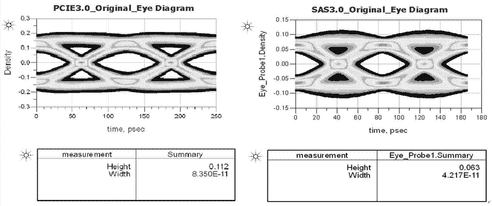
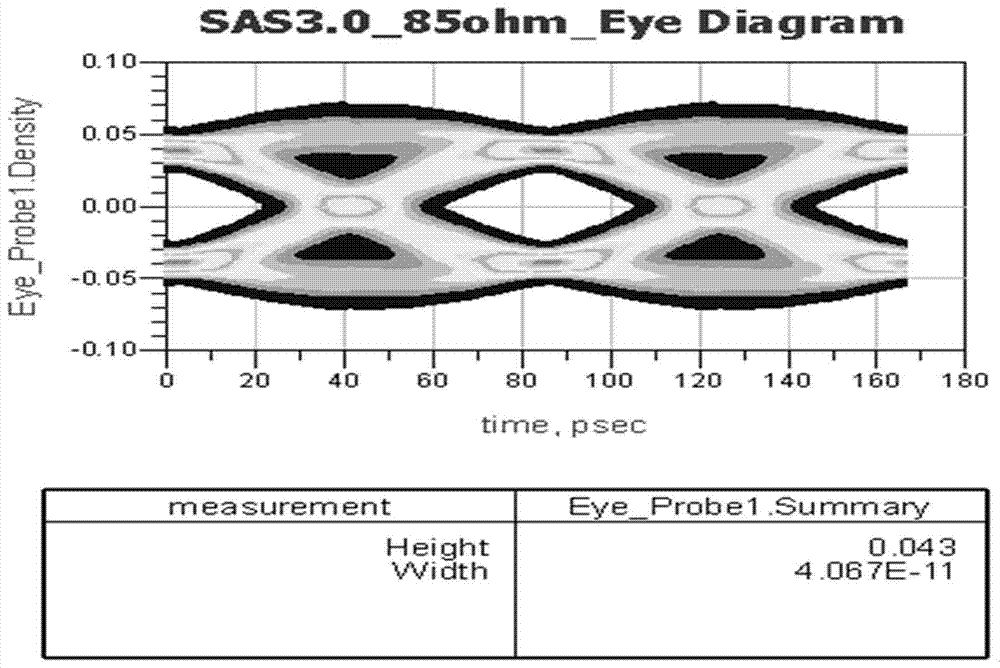
[0026] The signal lines with different impedance values ​​refer to SAS3.0 signal lines with trace impedance values ​​of 100 ohm and PCIE signal lines with 85 ohms. Correspond...


PUM


Abstract

The invention discloses a routing common method for different impedance signal lines and a PCB board. The method comprises the steps that signal lines of different impedance values on the PCB board are connected with Cap capacitors; a PCB Trace channel is shared by all cap capacitors; and the Cap capacitors are used as Bom selector switches for Bom switching, so that the routing of all signal lines on the PCB board are integrated. Compared with the prior art, the routing common method for different impedance signal lines and the PCB board have the advantages that the scheme that the transmission channel on the PCB board is shared by buses of different impedance values is used to reduce the number of high speed routing on the board; the function of each bus of a product is realized, and the size, the area and the number of layers of the board are reduced; the development cost of the board is reduced; the market competitiveness of the product is enhanced; and the practicability is high.

Description

technical field [0001] The invention relates to the technical field of PCB wiring, in particular to a method for realizing common routing of signal lines with different impedances and a PCB board. Background technique [0002] With the rapid development of the electronics industry, the design of the server motherboard is developing in the direction of high density and high speed. The size of the PCB board structure is reduced, and the number and speed of the high-speed IO ports output by the CPU chip are greatly increased, so as to enhance the competitiveness of the product in the market. . [0003] However, as the number of IO ports increases, it also means that the number of high-speed signal lines to be routed on the PCB board will increase exponentially. For example, the original CPU only supports one PCIEx16 port, which means that the PCB wiring needs to route 16 pairs of differential lines for each of the PCIE TX and RX channels, and a total of 32 pairs of wiring. Wh...

Claims


Application Information

Patent Timeline
IPC IPC(8): H05K1/02
CPCH05K1/0231H05K1/0228H05K1/0296H05K2201/09227
Inventor 武宁
Owner ZHENGZHOU YUNHAI INFORMATION TECH CO LTD
Why Eureka
Try Eureka