A detection device and method for distinguishing and recording the position of a silicon wafer

A detection device and silicon wafer technology, applied in measurement devices, optical devices, program-controlled manipulators, etc., to achieve the effects of ensuring quality, reducing verification time, and shortening action time

Active Publication Date: 2019-08-09
BEIJING UNIV OF TECH
View PDF5 Cites 0 Cited by
  • Summary
  • Abstract
  • Description
  • Claims
  • Application Information

AI Technical Summary

Problems solved by technology

[0005] In order to solve the problem that traditional infrared scanning is prone to large errors in identifying the position of thin silicon wafers, the present invention provides a detection device and method for identifying and recording the position of silicon wafers. The technical solutions adopted are as follows:

Method used


Image

  • A detection device and method for distinguishing and recording the position of a silicon wafer
  • A detection device and method for distinguishing and recording the position of a silicon wafer
  • A detection device and method for distinguishing and recording the position of a silicon wafer

Examples


Embodiment Construction

[0024] The present invention will be further described below in conjunction with accompanying drawing:

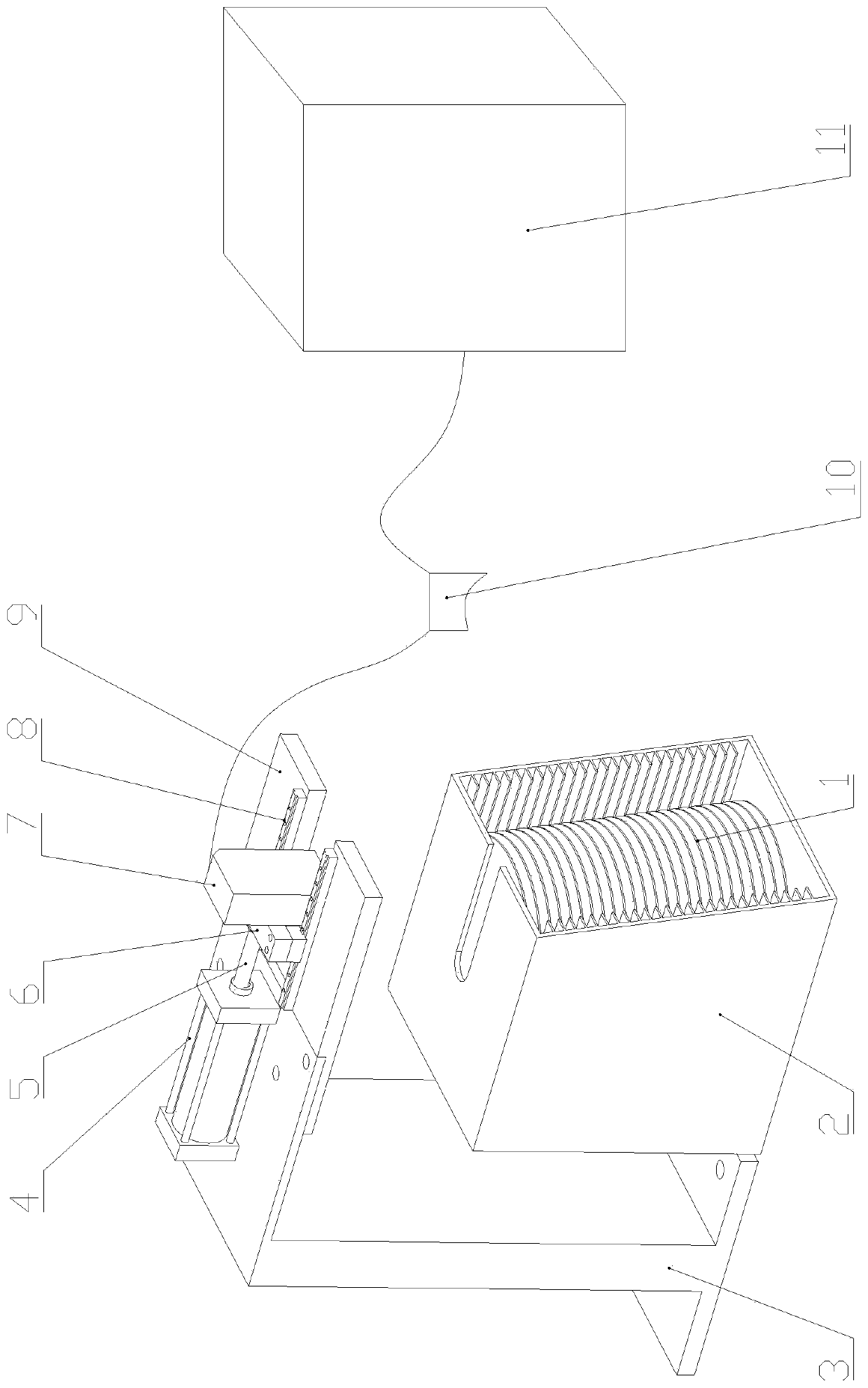
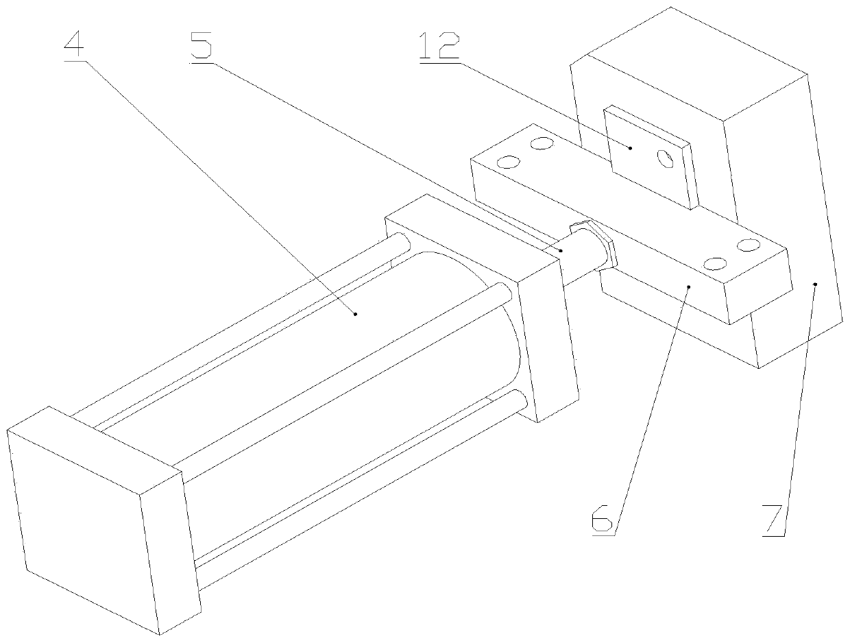
[0025] figure 1 Schematic diagram of the detection device for identifying and recording the silicon wafer position. The device is composed of two parts: a mechanical structure module and a signal acquisition module. The mechanical structure module includes a silicon chip (1), a silicon chip box (2), a vertical support (3), a horizontal support (9), a cylinder body (4), a cylinder piston (5), a horizontal guide rail (8), and a sensor Connecting plate (12) and slider beam (6). The signal acquisition module includes an infrared distance sensor (7), an acquisition card (10) and an industrial computer (11).

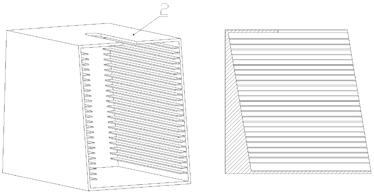
[0026] The silicon wafer (1) is placed in the silicon wafer box (2) according to the slot position, the silicon wafer box (2) and the vertical support (3) are on the same working plane, and the vertical support (3) is installed on the working plane by bolts Above, the h...


PUM


Abstract

A detection device and method for differentiating and recording the position of a silicon wafer (1). Slots of a silicon wafer box (2) are arranged in a trapezoidal manner, and the upper end thereof is provided with an opening, so that the edge of silicon wafers (1) at each layer may be observed when the silicon wafers are viewed from top to bottom; and an infrared distance sensor (7) is installed above the silicon wafer box (2); a signal transmitting path is along the vertical direction; an air cylinder (4) drives the sensor (7) to move in a straight line, and a signal transmitting diode of the sensor (7) transmits a signal to the silicon wafers (1) by means of an opening at the upper end of a silicon wafer box (2); signals are reflected by the edge of the silicon wafers (1) at each layer and received by a receiving diode; signals reflected by the silicon wafers (1) which are located at different layers are different, and the reflected signals are transmitted to an industrial personal computer (11) by means of an acquisition card (10); the industrial personal computer (11) analyzes and classifies the acquired signals by means of software, and a manipulator performs process operations according to data of the industrial personal computer (11).

Description

technical field [0001] The invention relates to a detection device and method for distinguishing and recording the position of a silicon wafer, and specifically relates to the technical field of semiconductor handling equipment. Background technique [0002] Silicon wafers are widely used in semiconductor components, and their fineness represents the manufacturing process level of semiconductors. During the manufacturing process of silicon wafers, there are strict requirements on the environment, processing and carrying devices. Silicon wafers are generally stored in silicon wafers. In the box, the robotic arm will grab and carry the silicon wafers from the box for process processing. [0003] The silicon wafer box is generally placed vertically, and the front opening is used for the robot to grab and store the silicon wafer. There are layers of slots distributed in the silicon wafer box, and each slot places a silicon wafer. There are usually 25 slots in the box. The slots...

Claims


Application Information

Patent Timeline
Patent Type & Authority Patents(China)
IPC IPC(8): G01B11/00B25J9/12
CPCB25J9/12G01B11/002
Inventor 刘志峰陶文秀杨聪彬王冰文俊武
Owner BEIJING UNIV OF TECH
Why Eureka
Try Eureka