Super junction power device and manufacturing method thereof

A technology of power devices and super junctions, which is applied in semiconductor/solid-state device manufacturing, semiconductor devices, electrical components, etc., can solve the problem of destroying the charge balance at the bottom of the columnar epitaxial doped region, reducing the bottom width, and the breakdown voltage of super junction power devices. Reduce and other problems to achieve the effect of improving reverse recovery characteristics, easy charge balance, and vertical super junction area

Active Publication Date: 2017-09-05
SUZHOU ORIENTAL SEMICONDUCTOR CO LTD
View PDF5 Cites 3 Cited by
  • Summary
  • Abstract
  • Description
  • Claims
  • Application Information

AI Technical Summary

Problems solved by technology

However, this technology has the following disadvantages. Since the sidewalls of the columnar epitaxial doped regions usually have inclined angles, the width of the bottom of the columnar epitaxial doped regions becomes smaller, ther

Method used


Image

  • Super junction power device and manufacturing method thereof
  • Super junction power device and manufacturing method thereof
  • Super junction power device and manufacturing method thereof

Examples


Embodiment Construction

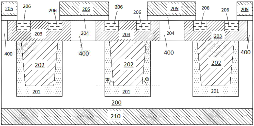
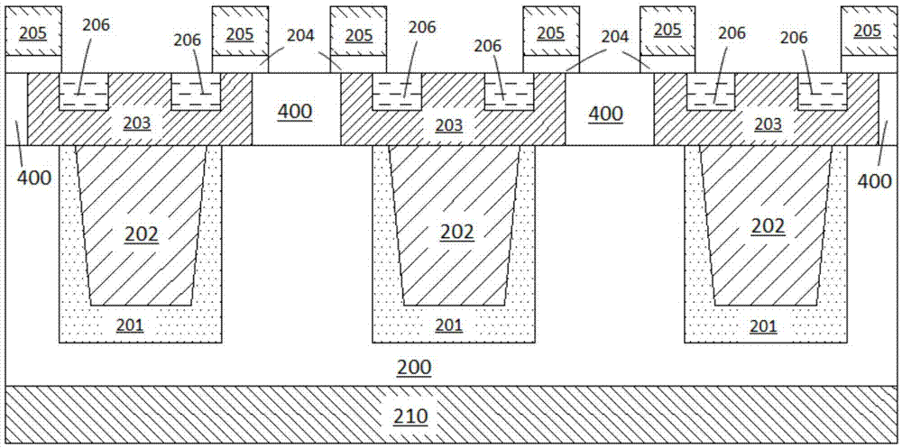
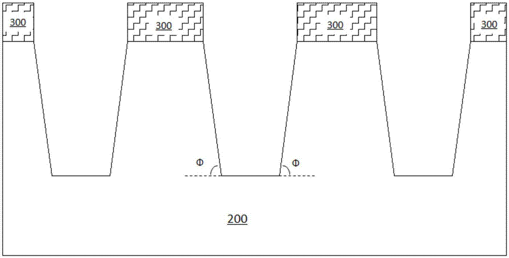
[0032] The present invention will be further described in detail below in conjunction with the accompanying drawings, so that those skilled in the art can implement it with reference to the description.

[0033] It should be understood that terms such as "having", "comprising" and "comprising" used herein do not denote the presence or addition of one or more other elements or combinations thereof.

[0034] At the same time, in order to clearly illustrate the specific implementation of the present invention, the schematic diagrams listed in the accompanying drawings of the description magnify the thicknesses of the layers and regions described in the present invention, and the sizes of the listed figures do not represent actual sizes; the accompanying drawings of the description are schematic should not limit the scope of the present invention. The embodiments listed in the description should not be limited to the specific shapes of the regions shown in the drawings of the desc...


PUM


Abstract

A super junction power device disclosed by the invention comprises a substrate epitaxial layer of a first doping type, body regions of a second doping type, and JFET regions. The substrate epitaxial layer is internally provided with a drain region of the first doping type and a plurality of sidewall-sloped columnar epitaxial doped regions of the second doping type. The body regions are respectively arranged on the top ends of the columnar epitaxial doped regions, and each body region is internally provided with source regions of the first doping type. Each JFET region is disposed between every two adjacent body regions. A gate oxide layer is arranged on the body regions and the JFET regions. Gates are arranged on the gate oxide layer. Compensation injection regions are arranged in the substrate epitaxial layer at the two sides of the sidewalls and at the bottom of the columnar epitaxial doped regions. The breakdown voltage is increased and the reverse recovery characteristic is improved under the condition that the on resistance of the super junction power device is basically unchanged. The manufacturing process is simple and easy to implement.

Description

technical field [0001] The invention belongs to the technical field of semiconductor power devices, in particular to a super junction power device and a manufacturing method thereof. Background technique [0002] The super junction power device forms a plurality of columnar epitaxial doped regions in the substrate epitaxial layer. The columnar epitaxial doped regions and the substrate epitaxial layer have the opposite doping type. Between the columnar epitaxial doped regions and the substrate epitaxial layer Carriers are easy to deplete each other to increase the breakdown voltage of super junction power devices. In the prior art, the manufacturing method of super-junction power devices is usually to first grow one or two layers of substrate epitaxial layer, then form trenches in the substrate epitaxial layer, and then grow the substrate epitaxial layer material so that in the trench A columnar epitaxial doped region is formed inside. The technical disadvantage of the exis...

Claims


Application Information

Patent Timeline
IPC IPC(8): H01L29/78H01L29/06H01L21/336
CPCH01L29/0634H01L29/0684H01L29/66666H01L29/7828
Inventor 刘磊龚轶袁愿林刘伟
Owner SUZHOU ORIENTAL SEMICONDUCTOR CO LTD
Why Eureka
Try Eureka