Supercharge Your Innovation With Domain-Expert AI Agents!

Printed circuit board product with antenna structure and method for its production

A technology of printed circuit board and antenna structure, applied in the directions of printed circuit, printed circuit, printed circuit manufacturing, etc., can solve the problems of long signal line, complex chip packaging and lamination, etc., and achieve the effect of depth and flexibility

Active Publication Date: 2017-09-05
AT & S AUSTRIA TECH & SYSTTECHN AG
View PDF10 Cites 4 Cited by
  • Summary
  • Abstract
  • Description
  • Claims
  • Application Information

AI Technical Summary

Problems solved by technology

On the downside, the buildup of the chip package is complex and - since the reflector is positioned offset from the antenna - it is not suitable for use with standard laminate materials which are often used for low cost manufacturing such as based on FR-4 laminate
Another disadvantage is the length of the signal line because the IC device is mounted on the opposite ground plane side of the antenna

Method used


Image

  • Printed circuit board product with antenna structure and method for its production
  • Printed circuit board product with antenna structure and method for its production
  • Printed circuit board product with antenna structure and method for its production

Examples


Embodiment Construction

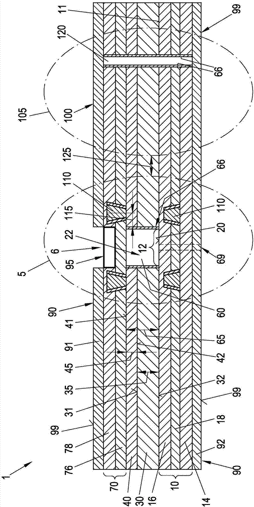
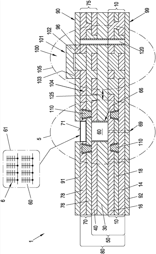
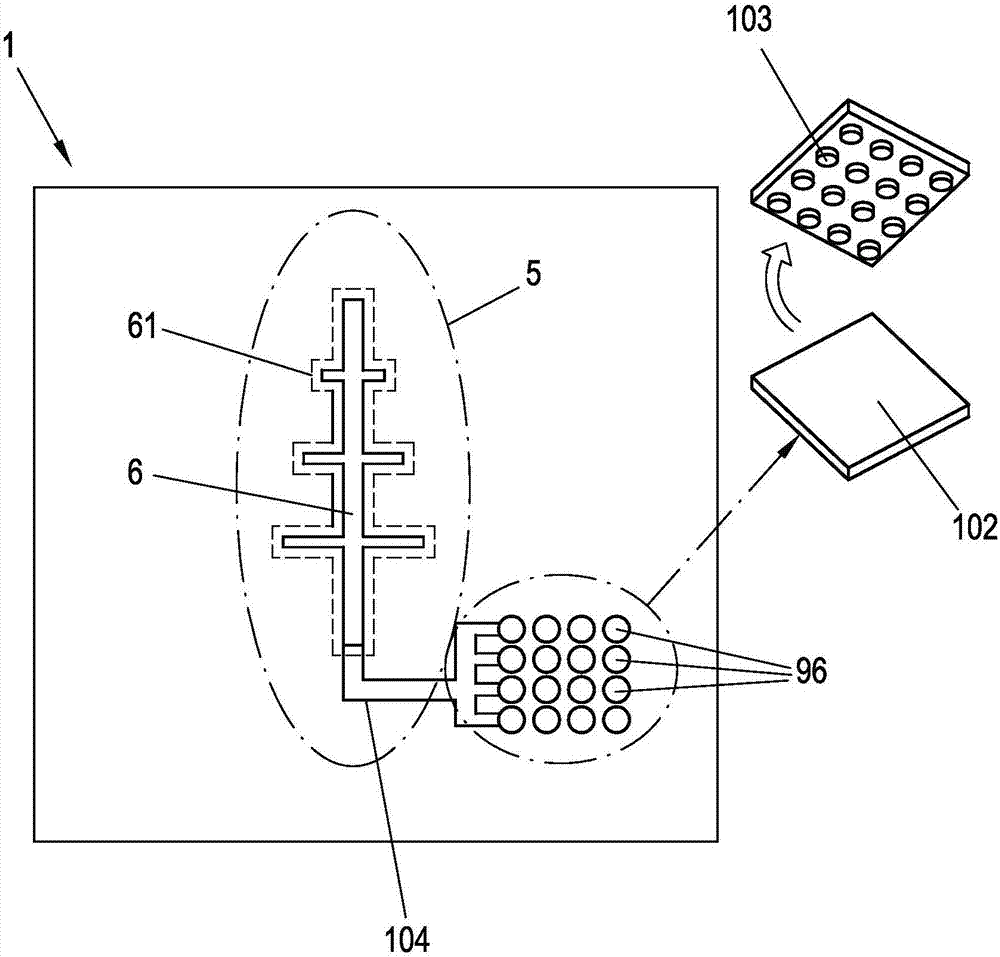
[0097] In the disclosed schematic diagrams, for ease of understanding, in addition to those diagrams that clearly show the conductive paths of the structured conductive layers connected by vias, the conductive layer is most often shown as a flat continuous conductive layer. Therefore, those drawings that schematically show continuous conductive layers without structured conductive paths and respective vias, micro-vias, plated through holes, etc., which connect the conductive layer, are not shown to be those skilled in the art. Known electrical functions. Those skilled in the art also know how to design and structure the conductive layer according to a specific task to obtain an appropriate conductive path. The main purpose of the drawings is to exemplify the corresponding layer structure in the production of an intermediate printed circuit board product according to the present invention in a schematic way. It is emphasized that the drawings are not shown to true scale, as for...


PUM


Abstract

A method for producing an intermediate printed circuit board product with an antenna structure, including steps of providing a ground layer including optionally a release layer that is removably positioned on an antenna subarea of an exterior side of the ground layer; attaching a dielectric insulating layer on the exterior side of the ground layer that is if applicable partly covered by the release layer; attaching a conducting layer on an exterior side of the dielectric insulating layer; laminating of the layers to receive a first semi-finished product; manufacturing of an antenna cavity throughout the conducting layer and the dielectric insulating layer with a ground-plane area that is if applicable made up of the release layer; attaching a compound signal layer on the conducting layer covering the antenna cavity; and laminating of the layers to receive the intermediate product.

Description

Technical field [0001] The present invention relates to a method for producing an intermediate printed circuit board product having an antenna structure for high frequency applications. The invention also relates to an intermediate printed circuit board product and a printed circuit board with an antenna structure. Background technique [0002] Once the operating frequency is increased to 500 MHz and above, the choice of laminates generally available to designers for manufacturing printed circuit boards (PCBs) is significantly reduced. [0003] Disadvantageously, standard laminate materials often used for low-cost manufacturing of printed circuit boards, such as FR-4 based laminates, have relatively high relative permittivities, with a dielectric constant DC approximately in the range between 4.3 and 5.4. FR-4 (or FR4) is the grade designation for glass fiber reinforced epoxy laminates, tubes, rods, and printed circuit boards (PCB). FR-4 named a composite material composed of wov...

Claims


Application Information

Patent Timeline
Patent Type & Authority Applications(China)
IPC IPC(8): H05K3/46H05K1/02H05K1/16H01Q1/44H01Q1/38
CPCH01Q1/38H01Q1/44H05K1/0219H05K1/0298H05K1/16H05K3/4688H05K3/4697H05K2201/0723H05K2201/0929H01Q19/10H05K2201/10098H01Q1/48H05K1/0222H05K1/115H05K1/185H05K3/282H05K3/4038H05K3/4644H05K2203/06
Inventor E·施拉费尔
Owner AT & S AUSTRIA TECH & SYSTTECHN AG
Features
  • R&D
  • Intellectual Property
  • Life Sciences
  • Materials
  • Tech Scout
  • Unparalleled Data Quality
  • Higher Quality Content
  • 60% Fewer Hallucinations
Learn More