Thin film transistor and manufacturing method thereof and display device

A technology of thin film transistors and active layers, which is applied in the direction of transistors, semiconductor/solid-state device manufacturing, and electric solid-state devices, etc. It can solve problems such as disconnection of metal wires in the source and drain layers, thick interlayer dielectric layers, and fractures, etc., to achieve It is not easy to break, improves the yield rate, and has the effect of strong flexibility

Active Publication Date: 2017-09-15
BOE TECH GRP CO LTD
View PDF5 Cites 5 Cited by
  • Summary
  • Abstract
  • Description
  • Claims
  • Application Information

AI Technical Summary

Problems solved by technology

[0004] The object of the present invention is to provide a thin film transistor, its manufacturing method and display device, which are used to solve the problem that in the existing flexible display screen, the thickness of the i

Method used


Image

  • Thin film transistor and manufacturing method thereof and display device
  • Thin film transistor and manufacturing method thereof and display device
  • Thin film transistor and manufacturing method thereof and display device

Examples


Example Embodiment

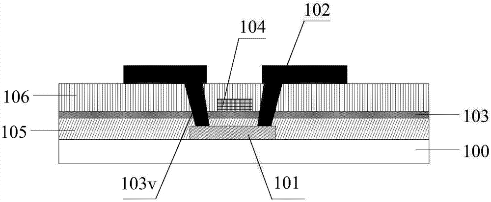
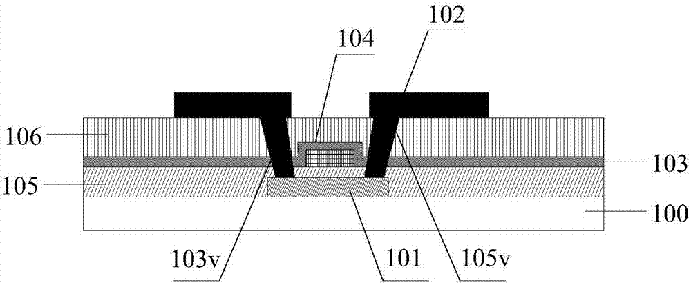
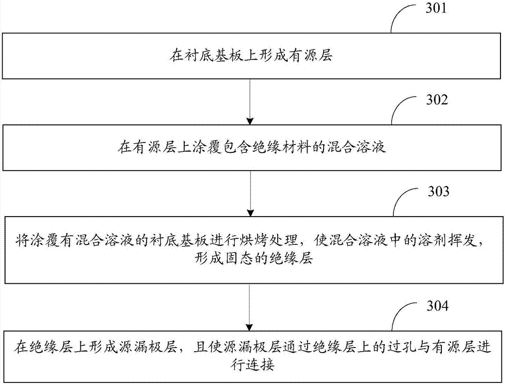
[0031] The following will clearly and completely describe the technical solutions in the embodiments of the present invention with reference to the accompanying drawings in the embodiments of the present invention. Obviously, the described embodiments are only some, not all, embodiments of the present invention. Based on the embodiments of the present invention, all other embodiments obtained by persons of ordinary skill in the art without making creative efforts belong to the protection scope of the present invention.

[0032] The thickness and area size and shape of each film layer in the drawings do not reflect the true proportion of the thin film transistor, and the purpose is only to schematically illustrate the content of the present invention.

[0033] A thin film transistor provided by an embodiment of the present invention is redesigned and optimized on an existing thin film transistor, and an insulating layer made of a hydrogen storage material is provided between the...


PUM

PropertyMeasurementUnit
Thicknessaaaaaaaaaa

Abstract

The invention relates to a thin film transistor and a manufacturing method thereof and a display device, and is used for solving the problems in the present flexible display screen that the metal wires of the source and drain layer are broken because of fracturing in the bending process due to high thickness of the interlayer dielectric layer. The thin film transistor comprises an underlying substrate, an active layer and the source and drain layer which are arranged on the underlying substrate and an insulating layer which is arranged between the active layer and the source and drain layer. The source and drain layer is connected with the active layer through the through holes on the insulating layer. The material of the insulating layer includes hydrogen storage material. According to the thin film transistor, the insulating layer manufactured by the hydrogen storage material is arranged between the active layer and the source and drain layer, and the hydrogen atoms stored in the insulating layer can be provided for the active layer so that subsequent manufacturing of the interlayer dielectric layer can be omitted. Meanwhile, the flexible insulating layer has higher flexibility in comparison with the interlayer dielectric layer manufactured by inorganic material and is not liable to break in bending so that the yield rate of the product can be enhanced.

Description

technical field [0001] The invention relates to the technical field of thin film transistors, in particular to a thin film transistor, a manufacturing method thereof and a display device. Background technique [0002] Traditional displays are flat-panel displays, which cannot be bent at will. The future trend is to present a large amount of information on flexible bodies, that is, to display on flexible displays, that is, to realize flexible displays. The official definition of a flexible display is a display device whose display screen and module can be mechanically bent in any step of substrate packaging, production, storage, use, operation, process connection, handling, and transportation. In the existing LTPS (Low Temperature Poly-silicon, low temperature polysilicon) backplane preparation process, the interlayer dielectric layer arranged between the gate and the active layer in the thin film transistor, because it generally uses the inorganic material SiO-SiNx The dou...

Claims


Application Information

Patent Timeline
IPC IPC(8): H01L29/786H01L21/336H01L27/12H01L21/77
CPCH01L27/1248H01L27/1292H01L29/66757H01L29/78606
Inventor 张帅李栋
Owner BOE TECH GRP CO LTD
Why Eureka
Try Eureka