Narrowband optical filter and film plating method thereof
A narrow-band filter and film stack technology, which is applied in optics, optical components, instruments, etc., can solve problems such as low image distortion, poor filter surface deformation, and large stress difference, so as to avoid deformation and reduce base Sheet deformation, coating cost reduction effect
- Summary
- Abstract
- Description
- Claims
- Application Information
AI Technical Summary
Problems solved by technology
Method used
Image
Examples
Embodiment 1
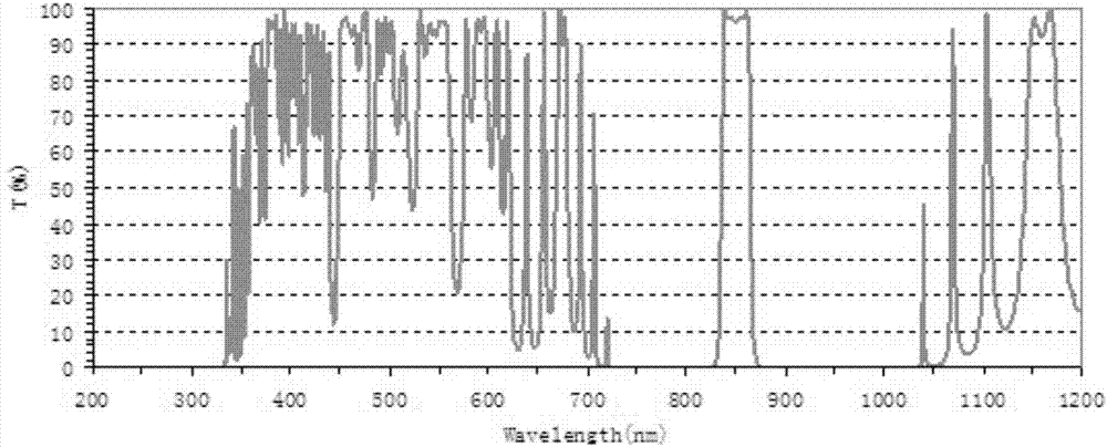
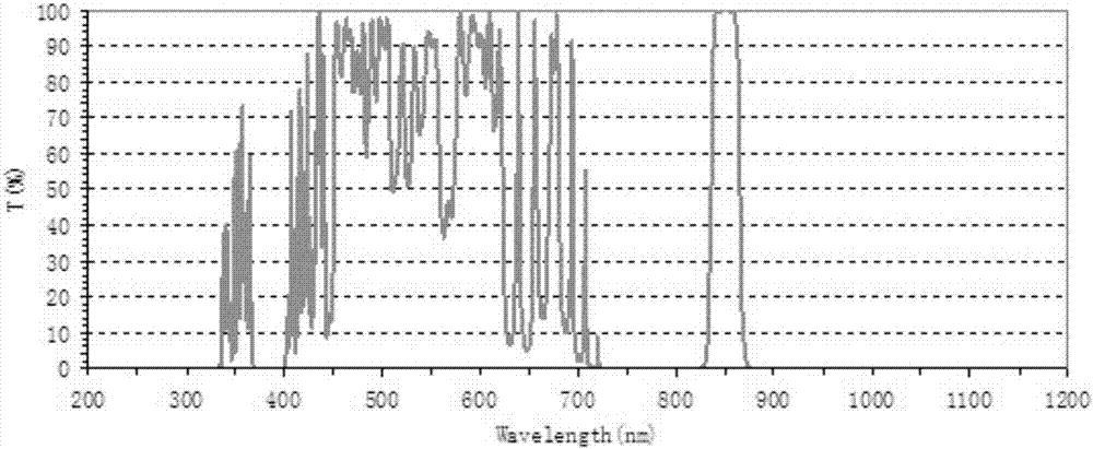
[0022] Taking the BP850 / 30 product as an example, the design center wavelength is 850nm, the bandwidth is 30nm, the cut-off depth is OD4, and the cut-off range is 200-1200nm.
[0023] Its preparation process is as follows:
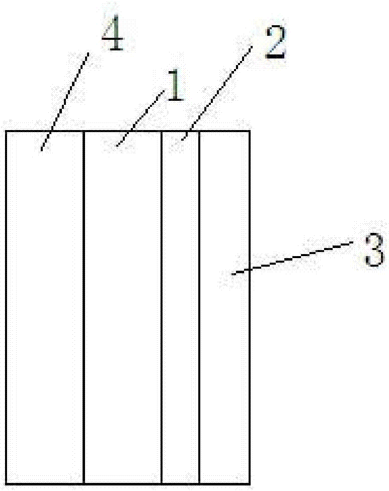
[0024] The first step is to design the main membrane stack 2 of the light control method, so that the refractive index of the equivalent substrate formed by the combination of the main membrane stack 2 and the glass substrate 1 is equivalent to that of the glass substrate 1 at 850 nm.
[0025] According to the optical thin film theory, the characteristic matrix for the calculation of optical multilayer film properties is:
[0026]
[0027]
[0028] no j is the refractive index of the jth film, d j is the physical thickness of the jth film, θ j is the incident angle of light in the jth film, λ is the reference wavelength, η j is the admittance of the thin film of the jth layer, η j =n j -ik j , when the film layer is a non-absorbing film, k j ...
PUM
 Abstract
Description
Claims
Application Information


