Cooling chamber and semiconductor processing equipment

A cooling chamber and cooling gas technology, which is applied in semiconductor devices, semiconductor/solid-state device manufacturing, electric solid-state devices, etc., can solve the problems of inability to meet equipment capacity requirements, low heat absorption efficiency of cooling chambers, and slow cooling speed of trays. Achieve good heat absorption performance, improve cooling efficiency, and increase productivity

Active Publication Date: 2017-09-22
BEIJING NAURA MICROELECTRONICS EQUIP CO LTD
View PDF9 Cites 7 Cited by
  • Summary
  • Abstract
  • Description
  • Claims
  • Application Information

AI Technical Summary

Problems solved by technology

[0005] However, due to the limitation of the heat absorption performance of the material (usually steel) of the cavity 102 and the upper cover 101, the heat absorption efficiency of the cooling chamber is low, resulting in a slow cooling rate of the tray, which cannot meet the production capacity requirements of the equipment.

Method used


Image

  • Cooling chamber and semiconductor processing equipment
  • Cooling chamber and semiconductor processing equipment

Examples


Embodiment Construction

[0027] In order for those skilled in the art to better understand the technical solution of the present invention, the cooling chamber and semiconductor processing equipment provided by the present invention will be described in detail below with reference to the accompanying drawings.

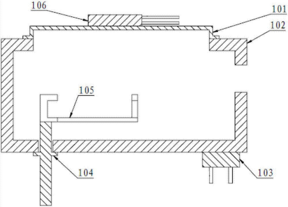
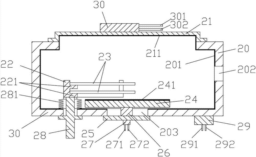
[0028] figure 2 A cross-sectional view of a cooling chamber provided for an embodiment of the present invention. see figure 2 , the chamber wall of the cooling chamber comprises a top wall 21, a side wall 20 and a bottom wall 30, the side wall 20 and the bottom wall 30 form an integrated cavity with an opening at the top, and the top wall 21 is arranged on the top of the integrated cavity , closing the top opening of the cavity. Wherein, a first cooling channel (not shown in the figure) is provided in the side wall 20 and the bottom wall 30 ; a third cooling channel (not shown in the figure) is provided in the top wall 21 . Moreover, a bracket 22 for carrying a tray 23 is arranged in the ...


PUM


Abstract

The invention provides a cooling chamber and semiconductor processing equipment. The chamber wall of the cooling chamber is internally provided with a first cooling channel, and the cooling medium is piped into the first cooling channel so as to cool the chamber wall. Besides, the cooling chamber is internally provided with a bracket which is used for bearing a tray, and the tray is used for bearing a processed workpiece. Furthermore, a black oxide layer is formed on at least partial internal surface of the chamber wall of the cooling chamber. According to the cooling chamber, the cooling efficiency of the tray can be enhanced so as to enhance the productivity of equipment.

Description

technical field [0001] The invention relates to the field of semiconductor manufacturing, in particular to a cooling chamber and semiconductor processing equipment. Background technique [0002] Physical vapor deposition (PVD) technology is the most widely used type of thin film manufacturing technology in the semiconductor industry, and generally refers to the thin film preparation process that uses physical methods to prepare thin films. In the PVD process, the deposition of most thin films requires the base to cool or heat the wafer, and its efficiency plays a vital role in the quality of deposited thin films. [0003] After the high-temperature process is completed, the tray used to carry the wafer needs to be lowered to a lower temperature in a vacuum before it is passed out of the process chamber and exposed to the atmosphere to ensure the quality of the deposited film and It is convenient for the operator to operate. In order to reduce the tray to a reasonable tempe...

Claims


Application Information

Patent Timeline
Patent Type & Authority Applications(China)
IPC IPC(8): H01L21/67H01L21/673
CPCH01L21/67011H01L21/673H01L2221/67H01L2221/683
Inventor 王桐武学伟张军董博宇郭冰亮王军张鹤南徐宝岗马怀超刘绍辉赵康宁耿玉洁王庆轩崔亚欣
Owner BEIJING NAURA MICROELECTRONICS EQUIP CO LTD
Why Eureka
Try Eureka