

Preparation method of wedge-shaped thin film
A wedge-shaped and thin-film technology is applied in the field of preparation of wedge-shaped thin films, which can solve the problems of forming cracks, affecting resonator performance and ESD reliability, and poor piezoelectric film performance, and achieving the effect of improving performance and reliability.
- Summary
- Abstract
- Description
- Claims
- Application Information
AI Technical Summary
Problems solved by technology
Method used
Image

Examples
Embodiment 1
[0026] Fig. 1 is the preparation process flowchart of a kind of wedge shape film of the embodiment of the present invention, and this preparation process comprises:
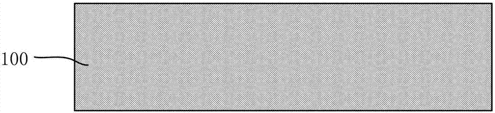
[0027] (a) Prepare a silicon wafer 100 polished on one or both sides, with the polished side up, and perform standard cleaning. As shown in Figure 1(a).
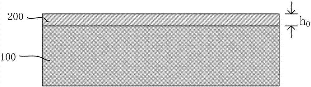
[0028] (b) Deposit film 200 on silicon wafer 100, for example film 200 is Mo; Its thickness is h 0 , such as 470nm. As shown in Figure 1(b).
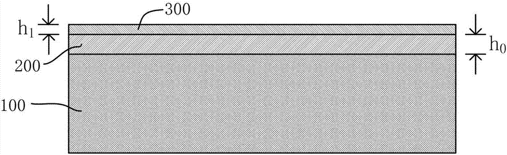
[0029] (c) Deposit a thin film 300 on the thin film 200, for example, the thin film 300 is A1; its thickness is h 1 , for example 160nm. As shown in Figure 1(c).
[0030] (d) throw photoresist 400 evenly on film 300, its thickness is h 2, such as 1um. As shown in Figure 1(d).
[0031] (e) Photolithography and development are performed on the photoresist to form the desired pattern. As shown in Figure 1(e).
[0032] (f) Under the protection of the aforementioned photoresist 400, the thin film 300 is etched, for ...
Embodiment 2
[0041] The present invention also proposes a thin-film bulk acoustic resonator, including the wedge-shaped structure formed in embodiment 1, such as forming a cavity on the substrate, forming a bottom electrode of the wedge-shaped structure on the cavity, and further depositing a voltage on the bottom electrode. Electrical material layer, top electrode. Since the piezoelectric material layer and the top electrode layer are prepared on the wedge-shaped structure, defects such as cracks in the subsequently grown thin film layer are effectively avoided, and the performance and reliability of the device are greatly improved.
PUM
 Abstract
Description
Claims
Application Information