Formation method of semiconductor structure

A semiconductor and isolation structure technology, applied in the field of semiconductor structure formation, can solve the problems such as the performance and reliability of the semiconductor structure need to be improved, and achieve the effects of less residue, smooth sidewall surface, and improved performance and reliability

Pending Publication Date: 2022-07-29
SEMICON MFG INT (SHANGHAI) CORP +1
View PDF0 Cites 0 Cited by
  • Summary
  • Abstract
  • Description
  • Claims
  • Application Information

AI Technical Summary

Problems solved by technology

[0003] However, the performance and reliability of exis

Method used


Image

  • Formation method of semiconductor structure
  • Formation method of semiconductor structure
  • Formation method of semiconductor structure

Examples


Example Embodiment

[0024] As mentioned in the background, the performance and reliability of existing semiconductor structures still need to be improved. The reasons why the performance and reliability of the semiconductor structure still need to be improved will be described in detail below with reference to the accompanying drawings.

[0025] Figure 1 to Figure 5 It is a schematic structural diagram of each step of a method for forming a semiconductor structure.

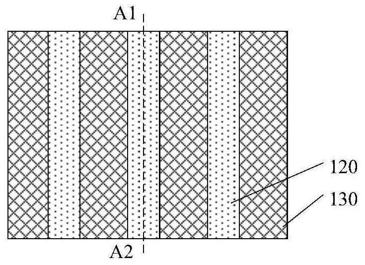
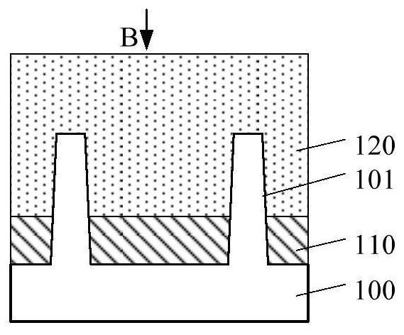
[0026] Please refer to figure 1 and figure 2 , figure 2 Yes figure 1 Schematic diagram of the cross-sectional structure along the direction A1-A2, figure 1 Yes figure 2 A schematic top view of the structure along the direction B in the middle, a substrate 100 is provided, and the substrate 100 has a plurality of fins 101 separated from each other; a first dielectric layer 110 is formed on the surface of the substrate 100, and the first dielectric layer 110 Covering part of the sidewall surface of the fin 101; forming a n...


PUM


Abstract

A method for forming a semiconductor structure comprises the steps that a substrate is provided, and the substrate is provided with a plurality of fin structures which are separated from one another; forming a plurality of first dummy gates crossing the fin structures on the substrate; a dielectric layer is formed on the substrate, the dielectric layer is further located on the side walls of the first dummy gates, and the top faces of the first dummy gates are exposed out of the surface of the dielectric layer; after the dielectric layer is formed, removing the plurality of first dummy gates, and forming a plurality of gate openings in the dielectric layer; forming a second dummy gate in the gate opening; a gate isolation structure is formed, the gate isolation structure penetrates through at least one second dummy gate in the first direction, and the first direction is perpendicular to the extending direction of the second dummy gate. Therefore, the performance and the reliability of the semiconductor structure are improved.

Description

technical field [0001] The present invention relates to the technical field of semiconductor manufacturing, and in particular, to a method for forming a semiconductor structure. Background technique [0002] With the continuous development of integrated circuit manufacturing technology, the feature size of MOS transistors is getting smaller and smaller. In order to reduce the parasitic capacitance of the MOS transistor gate and improve the device speed, the gate stack of the high-K gate dielectric layer and the metal gate is required. Structures are introduced into MOS transistors. In order to avoid the influence of the metal material of the metal gate on other structures of the transistor, the gate stack structure of the metal gate and the high-K gate dielectric layer is usually fabricated by a “gate last” process. [0003] However, the performance and reliability of existing semiconductor structures still need to be improved. SUMMARY OF THE INVENTION [0004] The techn...

Claims


Application Information

Patent Timeline
IPC IPC(8): H01L21/336H01L29/423H01L21/28
CPCH01L29/42356H01L21/28141H01L29/66803
Inventor 李波潘璋刘琳唐睿智
Owner SEMICON MFG INT (SHANGHAI) CORP
Why Eureka
Try Eureka