Printed circuit board device manufacture method
A technology for printed circuit boards and manufacturing methods, which is applied in the directions of printed circuit manufacturing, printed circuits, and assembling printed circuits with electrical components, can solve problems such as low manufacturing efficiency, improve welding efficiency, improve demolding efficiency, and avoid solder paste. The effect of uneven coating
- Summary
- Abstract
- Description
- Claims
- Application Information
AI Technical Summary
Problems solved by technology
Method used
Image

Examples
Embodiment Construction
[0063] Referring to the drawings, wherein like reference numerals represent like components, the principles of the present invention are exemplified when implemented in a suitable computing environment. The following description is based on illustrated specific embodiments of the invention, which should not be construed as limiting other specific embodiments of the invention not described in detail herein.
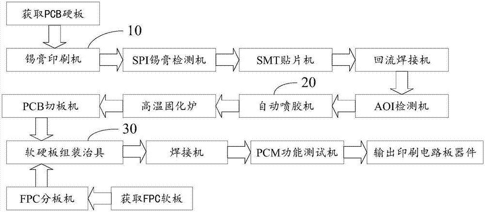
[0064] Please refer to figure 1 , figure 1 It is a schematic workflow diagram of the manufacturing method of the printed circuit board device of the present invention; the manufacturing method of the printed circuit board device of the present invention includes:
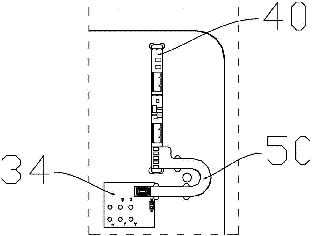
[0065] Obtain the PCB hard board 40, and determine the pad position on the PCB hard board 40;
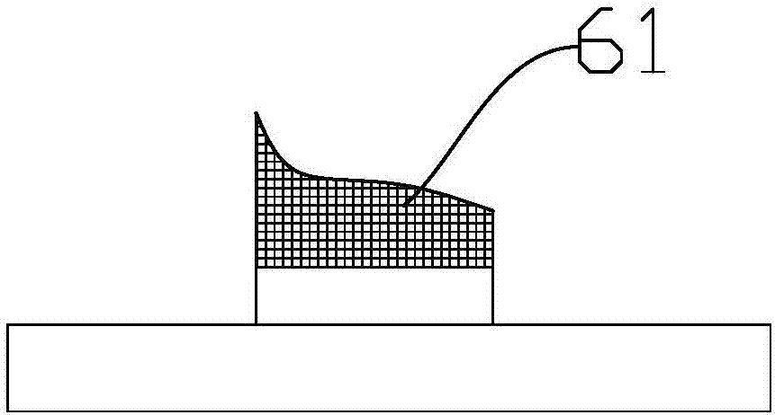
[0066] Use the solder paste printing machine 10 to apply solder paste 60 on the pad position on the PCB hard board 40;
[0067] Use the SPI solder paste inspection machine to detect whether the solder paste 60 on t...
PUM
 Abstract
Description
Claims
Application Information
 - Generate Ideas
- Intellectual Property
- Life Sciences
- Materials
- Tech Scout
- Unparalleled Data Quality
- Higher Quality Content
- 60% Fewer Hallucinations
Browse by: Latest US Patents, China's latest patents, Technical Efficacy Thesaurus, Application Domain, Technology Topic, Popular Technical Reports.
© 2025 PatSnap. All rights reserved.Legal|Privacy policy|Modern Slavery Act Transparency Statement|Sitemap|About US| Contact US: help@patsnap.com