Color film substrate and liquid crystal display panel

A technology of liquid crystal display panels and color film substrates, applied in nonlinear optics, instruments, optics, etc., can solve problems such as large noise, signal interference of touch sensing lines, static electricity, etc., and achieve the effect of solving signal interference

Inactive Publication Date: 2017-09-26
KUSN INFOVISION OPTOELECTRONICS
View PDF6 Cites 3 Cited by
  • Summary
  • Abstract
  • Description
  • Claims
  • Application Information

AI Technical Summary

Problems solved by technology

[0005] The purpose of the present invention is to provide a color filter substrate, which effectively solves the problem of static electricity caused by the absence of an outer ITO protective layer on the color filter substrate; at the same time, it can solve the problem of signal interference and excessive noise caused by the color filter substrate being matched with a touch sensing line

Method used


Image

  • Color film substrate and liquid crystal display panel
  • Color film substrate and liquid crystal display panel
  • Color film substrate and liquid crystal display panel

Examples


Embodiment 1

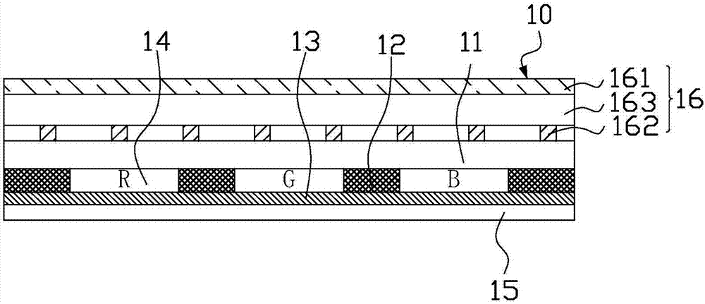
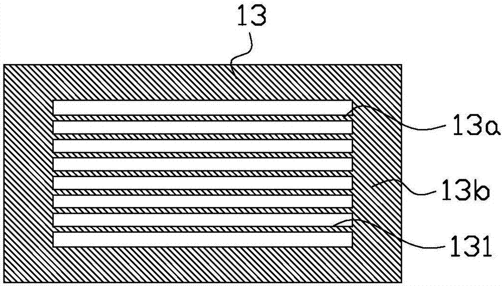
[0030] figure 1 It is a schematic structural diagram of a color substrate in a preferred embodiment of the present invention, figure 2 It is a schematic structural diagram of a conductive layer in a preferred embodiment of the present invention, image 3 is a schematic structural diagram of an array substrate in a preferred embodiment of the present invention, Figure 7 for figure 2 local schematic diagram. see figure 1 , figure 2 , image 3 and Figure 7 , the present invention provides a color filter substrate, including a substrate 11 , a black matrix 12 , a color resist layer 14 and a flat layer 15 are provided on the inner side of the substrate 11 , and a conductive layer 13 is also provided on the inner side of the substrate 11 . The conductive layer 13 is made of a transparent material such as indium tin oxide (ITO, Indium TinOxide) and other transparent conductive materials, but not limited thereto.

[0031] see figure 2 and image 3 The conductive layer ...

Embodiment 2

[0036] figure 1 It is a schematic structural diagram of a color substrate in a preferred embodiment of the present invention, image 3 is a schematic structural diagram of an array substrate in a preferred embodiment of the present invention, Figure 4 It is a schematic structural diagram of a conductive layer in another preferred embodiment of the present invention, Figure 8 for Figure 4 local schematic diagram. see figure 1 , image 3 , Figure 4 and Figure 8 , the present invention provides a color filter substrate, including a substrate 11 , a black matrix 12 , a color resist layer 14 and a flat layer 15 are provided on the inner side of the substrate 11 , and a conductive layer 13 is also provided on the inner side of the substrate 11 . The conductive layer 13 is made of a transparent material such as indium tin oxide (ITO, Indium TinOxide) and other transparent conductive materials.

[0037] see image 3 and Figure 4 The conductive layer 13 includes a first...

Embodiment 3

[0042] figure 1 It is a schematic structural diagram of a color substrate in a preferred embodiment of the present invention, image 3 is a schematic structural diagram of an array substrate in a preferred embodiment of the present invention, Figure 5 It is a schematic structural diagram of the conductive layer of another preferred embodiment of the present invention. Figure 9 for Figure 5 local schematic diagram. see figure 1 , Figure 5 and Figure 9 , the present invention provides a color filter substrate, including a substrate 11 , a black matrix 12 , a color resist layer 14 and a flat layer 15 are provided on the inner side of the substrate 11 , and a conductive layer 13 is also provided on the inner side of the substrate 11 . The conductive layer 13 is made of a transparent material such as indium tin oxide (ITO, Indium TinOxide) and other transparent conductive materials.

[0043] see image 3 and Figure 5 The conductive layer 13 includes a first conductiv...


PUM


Abstract

The invention provides a color film substrate and a liquid crystal display panel. The color film substrate comprises a lining, and the inner side of the lining is provided with a black matrix and a color resistor layer. The outer side of the lining is provided with a touch sensing circuit, the inner side of the lining is provided with a conductive layer which comprises a first conductive portion and a second conductive portion, the first conductive portion and the second conductive portion cover a display area and a non-display area respectively and connected into a whole, and the first conductive portion is in a hollowed-out structure while the second conductive portion is in a planar structure. The color film substrate has advantages that the problem of static electricity caused by lack of an ITO (indium tin oxide) protective layer on the outer side of an existing color film substrate is solved effectively, and problems of high noise and signal interference in joint use of the color film substrate and the touch sensing circuit can be solved as well.

Description

technical field [0001] The invention relates to the technical field of liquid crystal display, in particular to a color filter substrate and a liquid crystal display panel. Background technique [0002] Generally, an ITO protective layer is formed on the outside of the color filter substrate, which can play a role of shielding signals. However, when the LCD panel is formed with a touch panel on the outside of the color filter substrate, the touch panel on the outside of the color filter substrate is generally designed with a metal mesh. At this time, the ITO protective layer will interfere with the metal mesh. Interference, usually designed to remove the ITO protective layer. [0003] In some liquid crystal display panels, a gate driving circuit is integrated on an array substrate (Gate IC in Array, GIA), and such a gate driving integrated circuit is called a GIA circuit. The application of the GIA circuit reduces the driving cost. [0004] However, since the liquid cryst...

Claims


Application Information

Patent Timeline
Patent Type & Authority Applications(China)
IPC IPC(8): G02F1/1333G02F1/1335
CPCG02F1/1333G02F1/133308G02F1/133345G02F1/13338G02F1/133512G02F1/133334
Inventor 房耸井晓静王金烨李红侠
Owner KUSN INFOVISION OPTOELECTRONICS
Why Eureka
Try Eureka